1-2-6 High Voltage 3-Phase Brushless Motor Driver ICs
SLA6845M
Supports 3 Shunt, IGBT Output Element, Built-in Thermal Sensor and 7.5 V Regulator
■Features
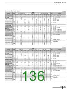
■Absolute Maximum Ratings
(Ta=25°C)
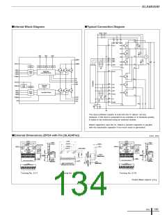
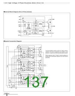
• A package including 6 units each of IGBT and
FRD for 3-phase bridge, and pre-drive (HVIC,
LVIC)
Parameter
IGBT Output Breakdown Voltage
Main Supply Voltage
Symbol
VCES
VBB
Ratings
600
450
20
20
3
6
35
–0.5 to +7
32.8
3.8
5.4
–20 to +100
150
Unit
V
V
V
V
A
A
mA
V
W
°C/W
°C/W
°C
°C
°C
ꢀConditions
Between VBB and GND
Between VCC and COM
Between VB and HS (U, V, W)
Tc=25°C
Control Supply Voltage
Vcc
• Best for driving a washing machine drying fan
motor
Control Supply Voltage (Bootstrap)
Output Current (continuous)
Output Current (pulse)
VBS
Io
Iop
• High side drive of bootstrap method has been
employed.
PW<100µs
Regulator Output Current
Input Voltage
IREG
VIN
• Built-in undervoltage lock out circuit (auto
regression)
Power Dissipation
PD
Tc=25°C, all IGBT elements in operation
All IGBT elements in operation
Thermal Resistance (IGBT Junction to Case)
Thermal Resistance (FRD Junction to Case)
Operating Case Temperature
Junction Temperature
Rj-c(I)
Rj-c(F)
TOP
Tj
All FRD elements in operation
• Built-in thermal sensor (non-stop)
• Built-in fail signal output function (when
operating the thermal sensor and undervoltage
lock out circuit)
Storage Temperature
Tstg
–40 to +150
• Support for 3-shunt current sense
• Built-in 7.5 V regulator output (35mA max.)
■Recommended Operating Conditions
Ratings
Parameter
Symbol
Unit
Conditions
min.
–
typ.
300
–
max.
Main Supply Voltage
VBB
Vcc
tdead
tocp
Cs
450
16.5
–
V
V
µs
µs
µF
°C
Between VBB and LS
Control Supply Voltage
Input Signal Dead Time
Overcurrent Protection Time
Snubber Capacitor
13.5
1.5
–
Between VCC and COM
Between LS1 to 3 and COM
–
–
2.0
0.1
125
0.01
–
–
Between VCC and COM
Junction Temperature
Tj
–
■Electrical Characteristics
(Ta=25°C)
Ratings
typ.
4
Parameter
Control Supply Current
Input Voltage
Symbol
Unit
mA
V
Conditions
min.
–
max.
6
2.5
–
Icc
VIH
Vcc=15V, VIN=5V
Vcc=15V, Output:ON
Vcc=15V, Output:OFF
Vcc=15V
–
2
VIL
1
–
1.5
0.5
50
Input Voltage Hysteresis Width
Input Current
VIhys
IIH
–
V
–
100
2
Vcc=15V, VIN=5V
Vcc=15V, VIN=0V
µA
IIL
–
–
VUVHL
VUVHH
VUVhys
VUVLL
VUVLH
VUVhys
VFOL
VFOH
TDH
9.0
9.5
–
10.0
10.5
0.5
11.0
11.5
0.5
–
11.0
11.5
–
Between VB and U (V, W)
Undervoltage Lock Out (high side)
V
Hystersis
10.0
10.5
–
12.0
12.5
–
Between VCC and COM
Undervoltage Lock Out (low side)
FO Terminal Output Voltage
V
V
Hystersis
Vcc=15V, IFO=–1mA
Vcc=15V, IFO=1.6mA
0
1.0
5.5
165
135
–
4.0
135
105
–
–
150
120
30
7.5
–
Thermal Protection and Release Threshold
TDL
°C
Vcc=15V, No Fin, IREG=0mA
TDhys
VREG
VCES
ICES
VCE(sat)
VF
Regulator Output Voltage
6.75
600
–
8.25
–
V
V
mA
V
V
ns
IREG=35mA
IGBT Output Breakdown Voltage
IGBT Output Leakage Current
IGBT Output Saturation Voltage
Diode Forward Voltage
Vcc=15V, Ic=1mA, VIN=0V
Vcc=15V, VCE=600V, VIN=0V
Vcc=15V, Ic=3A, VIN=5V
Vcc=15V, IF=3A, VIN=0V
IF=3A, di/dt=100A/µs
–
1
2.1
2.0
–
1.75
1.65
50
–
Diode Reverse Recovery Time
trr
td(on)
tr
td(off)
tf
td(on)
tr
td(off)
tf
–
–
315
50
375
165
325
60
–
–
–
–
–
–
–
–
High Side Switching Time
Low Side Switching Time
ns
ns
–
–
VBB=300V, Vcc=15V, Ic=3A, VIN=0 to 5V,
Inductive load
–
–
-
-
400
165
ICs
132

 ETC [ ETC ]