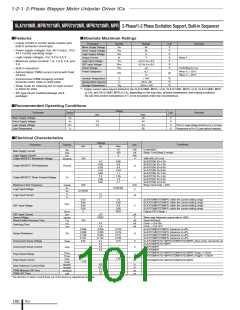
SLA7080MPR/7081MPR/7082MPR/7083MPR
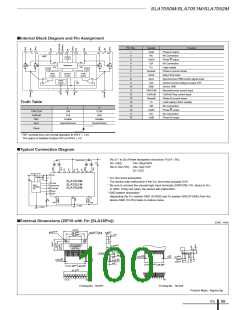
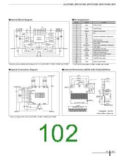
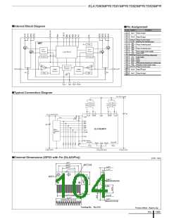
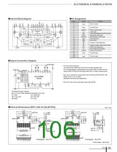
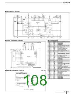
■Internal Block Diagram
■Pin Assignment
Pin No. Symbol
Function
1
2
Out A
Phase A output
3
4
5
6
7
/Out A Phase A output
Sense A
B_SEL
INA
Phase A current sense
Blanking time switching input
Phase A switching input
8
/INA
9
INB
/INB
Phase B switching input
10
11
12
VBB
Driver supply (motor supply)
Device GND
Gnd
13 Ref/Sleep
Control current/Sleep setting input
Logic supply
Gnd1
14
15
16
17
18
19
20
21
22
23
VDD
Gnd1
Gnd2
Sync
Flag
Gnd2
PWM synchronous/asynchronous switching input
Protection circuit monitor output
Phase B current sense
Sense B
Phase B output
Phase B output
/Out B
Out B
■Typical Connection Diagram
■External Dimensions (ZIP23 with Fin [SLA23Pin])
(Unit : mm)
0.2
31
φ3.2 0.15×3.8
0.2
24.4
0.2
0.2
0.1
16.4
4.8
1.7
0.15
φ3.2
0.2
2.45
(Measured at the root)
4–(R1)
R-end
+0.2
0.65
–0.1
1
22×P1.27 0.5=27.94
+0.2
0.55
–0.1
0.2
31.3
0.7
4.5
(Including the resin burr)
(Measured at the tip)
Forming No. No.2151
Product Mass : Approx.6g
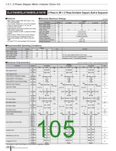
ICs
103

 ETC [ ETC ]