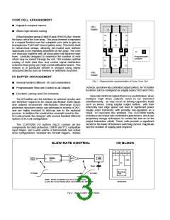
POWER SUPPLY DISTRIBUTION
■ Three power rings for good noise immunity
■ Optimized for efficient routing
Supply to
Core Logic
■ User defined placement of Power and Ground pads
VSS } Supply to
VDD } Intermediate
Buffers
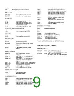
The power supply distribution scheme for the CLA70000
arrays (fig.3) has the flexibility to meet varying applications
needs. Three separate power rings are used, one each for the
internal core logic, intermediate buffer cells, and large output
driver cells. Noise generated in the low impedance output
drivers is isolated from the core logic and buffer areas. The
distribution of the supply rails can be automatically positioned
by the layout software which allows greater design flexibility
and optimisation.
VDD } Supply to
VSS
}
I/O Buffers
The power supply rings may be connected either to
separate pad locations or combined at a single location. All
I/O cell pads may be configured as either power or ground,
giving complete flexibility to the designer.
Fig 3. Power Supply Organisation
The CLA70000 arrays are built using the GEC Plessey 1
micron drawn CMOS process, which is the third generation of
our ‘V’ series process family. Manufacture is at GPS’s
Class10, 6-inch fabrication facility. The process is a twin well,
self aligned oxide-isolated technology on an epitaxial
substrate, with an effective channel length of 0.8 micron,
giving low defect density, high reliability, and inherently low
power dissipation. The process has excellent immunity to
latchup, and ESD, and exhibits stable performance
characteristics ideal for all commercial, industrial and military
applications.
PROCESS TECHNOLOGY
■ Advanced 1 micron twin well process with epitaxial
substrate
■ Class 10 six inch wafer fabrication facility
■ High density low power process
ABSOLUTE MAXIMUM RATINGS
RECOMMENDED MAXIMUM OPERATING LIMITS
Parameter
Min
Max
Units
Parameter
Min
Max
Units
Supply Voltage
Input Voltage
Output Voltage
ESD protection
Current per pad
Storage Temperature
Ceramic
-0.5
-0.5
-0.5
2.0
7.0
Vdd + 0.5
Vdd + 0.5
V
V
V
Supply Voltage
Input Voltage
Output Voltage
Operating Temperature
Commercial Grade
Industrial Grade
Military Grade
3.0
Vss
Vss
5.5
Vdd
Vdd
V
V
V
K Volts
mA
100
0
-40
-55
70
85*
125**
°C
°C
°C
-65
-40
150
125
°C
°C
Plastic
* 125°C maximum junction temperature for plastic devices.
**Subject to a maximum junction temperature of 150°C for
ceramic devices.
Operation outside these absolute maximum ratings may
permanently damage device characteristics and may affect
reliability.

 ETC [ ETC ]