MARCH 1992
2462 - 3.1
CLA70000 SERIES
HIGH DENSITY CMOS GATE ARRAYS
(Supersedes January 1992 edition - version 2.1)
Recent advances in CMOS processing technology and
OVERVIEW
improvements in design architecture have led to the
development of a new generation of array-based ASIC
products with vastly improved gate integration densities. This
family of CLA70000 1 micron CMOS arrays brings
considerable advantages to the design of next generation
systems combining high performance and high complexity.
The CLA70000 gate array family is GEC Plessey
Semiconductors' (GPS’s) sixth generation CMOS gate array
product. The family consists of nine arrays implemented on
the latest generation (1 micron) twin well epitaxial CMOS
process. The process in conjunction with the advanced layout
and route software, offers extremely high packing densities.
FEATURES
The array architecture is based upon the earlier well
proven CLA60000 series with the emphasis being placed on
high speed, high packing density, and provision of
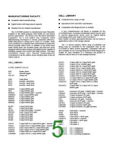
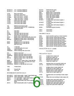
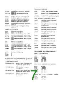
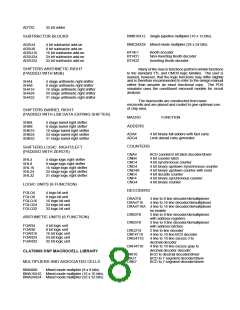
comprehensive cell libraries. The cell libraries encompass
new DSP and other specialized macros.
■ Low power channelless arrays from 5,000 to 250,000
available gates (5µW / gate / MHz)
■ 1 micron (0.8 micron effective) twin well epitaxial process
■ Typical gate delays of 400 ps (NAND2 , Fanout=2)
■ Comprehensive cell library including DSP, JTAG/BIST
and compiled memory cells (ROM blocks to 64K bits
and RAM blocks to 16K bits)
■ Extensive Range of Plastic and Ceramic Packages for
both Surface Mount and Through Board Assembly
■ Flexible I/O structure allows user to define power pad
locations
Fulldesignsupportisavailableformajorindustrystandard
ASIC design software tools, as well as GEC Plessey
Semiconductor’s proprietary PDS2 design environment.
Design support is provided by GEC Plessey Semiconductor’s
design centers, each offering a variety of design routes, which
may be customized to individual customer requirements.
■ Fully supported on industry standard workstations and
in-house software
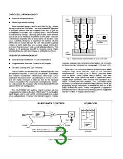
■ High drive output stages with slew rate control
■ Supports JTAG and BIST test philosophies (IEEE 1149-1
Test Procedures)
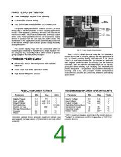
PRODUCT DETAILS
The CLA70000 array series is shown below with typical
figures given for usable gates. Actual gate utilization is
dependent on circuit structure, giving a range of 40 -70% for
two layer metallisation.
■ MIL 883C compliant product available (paragraph 1.2.1)
GATE
DEVICE
I/O AND
ESTIMATED
USABLE GATES
COMPLEXITY
NUMBER
POWER PADS
5K
CLA70000
CLA71000
CLA72000
CLA73000
CLA74000
CLA75000
CLA76000
CLA77000
CLA78000
44
2.5K
6K
12K
68
19K
84
9.5K
13.5K
17.5K
31.5K
49.5K
82K
27K
100
120
160
200
256
304
39K
70K
110K
182K
256K
115K

 ETC [ ETC ]