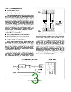
CORE CELL ARRANGEMENT
■ Supports compact macros
■ Allows high density routing
VSS
VDD
Supply
Supply
Afourtransistorgroup(2NMOSand2PMOS)(fig.1)forms
the basic cell of the core array. This array element is repeated
in a regular fashion over the complete core area to give an
homogenous ‘Full Field’ (sea of gates) array. This lends itself
to hierarchical design, allowing pre-routed user defined
subcircuits to be repeated anywhere on the array. The core
cell structure together with all associated cell libraries have
been carefully designed to maximize the number of nets
which may be routed through the cell. This enables optimal
routing of both data flow and control signal distribution
schemes thus giving very high overall utilization factors. This
feature is of particular benefit in designs using highly
structured blocks such as memory or arithmetic functions.
Programmable
contacts
VSS
VSS
Supply
Supply
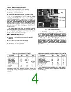
I/O BUFFER ARRANGEMENT
Fig 1. Diagrammatic representation of Array Core Cell
■ Several hundred different I/O cell combinations
■ Programmable Slew rate Control on all Outputs
controls, and slew rate controlled output buffers. All I/O buffer
locations can be configured as supply pads (VDD and VSS).
■ Excellent Latchup and ESD immunity
Slew rate control of output drivers is a useful feature when
multiple high drive outputs need to be switched
simultaneously, as may occur on driving capacitive loads
such as buses. Using regular output buffers with their
inherently fast edge speed can lead to significant power
supply noise transients, with possible mis-operation as a
result. To overcome this problem. The CLA70000 family
includes a set of slew rate controlled output drivers, which use
proprietary design techniques to control the turn-on of the
output transistors (di/dt). These cells provide a significant
benefit in the trade off between switching current magnitude
and the number of supply pads required.
The I/O buffers are the interface to external circuitry and
are therefore required to be robust and flexible. Both inputs
and outputs incorporate electrostatic discharge (ESD)
protection structures which can withstand in excess of 2KV,
and are highly resistant to latch-up due to the epitaxial
process. In addition the construction concepts used for the
I/O cells provide the designer with several hundred different
options of I/O cell configuration.
The CLA70000 I/O buffers (fig.2) contain all the
components for static protection, CMOS and TTL compatible
input stages, and a wide variety of intermediate and output
drive configurations. Included are Schmitt triggers, tristate
SLEW RATE CONTROL
I/O BLOCK
IB1 IB2 IB3 IB4 IB5
P
P
slew rate
controlled
driver
INPUT
DATA
OPT3
N
PIN
D
OP1
OP2
N
IP
50 pF
Bonding
Pad
2.5 Volts
2.5 Volts
IBSK1, IBSK2 and IBSK3 have been characterised
to give the correct timing when connected to the OPT* cells.
I/O BLOCK
Fig 2. Slew Control & I/O Block

 ETC [ ETC ]