ST90158 - EXTERNAL MEMORY INTERFACE (EXTMI)
EXTERNAL MEMORY SIGNALS (Cont’d)
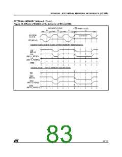
7.2.4 RW: Read/Write
Note: On some devices, the internal weak pull-up
is not present. In this case, an external one is
needed.
RW (Alternate Function Output, Active low,
Tristate) identifies the type of memory cycle:
RW=”1” identifies a memory read cycle, RW=”0”
identifies a memory write cycle. It is defined at the
beginning of each memory cycle and it remains
stable until the following memory cycle. RW is re-
leased in high-impedance during bus acknowl-
edge cycle or under processor control by setting
the HIMP bit (MODER). RW is enabled via soft-
ware as the Alternate Function output of the asso-
ciated I/O port bit (refer to specific ST9 device to
identify the port and pin). Under Reset status, the
associated bit of the port is set into bidirectional
weak pull-up mode.
The behavior of this signal is affected by the MC,
ETO and BSZ bits in the EMR1 register. Refer to
the Register description.
7.2.5 BREQ, BACK: Bus Request, Bus
Acknowledge
Note: These pins are available only on some ST9
devices (see Pin description).
BREQ (Alternate Function Input, Active low) indi-
cates to the ST9 that a bus request has tried or is
trying to gain control of the memory bus. Once en-
abled by setting the BRQEN bit (MODER.1,
R235), BREQ is sampled with the falling edge of
the processor internal clock during phase T2.
n
n
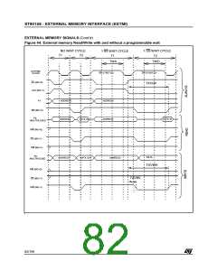
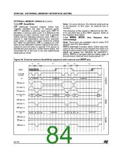
Figure 46. External memory Read/Write sequence with external wait (WAIT pin)
n
T2
T1
T2
T1
T2
T1
WAIT
SYSTEM
CLOCK
ADDRESS
ADDRESS
ADDRESS
P1
AS (MC=0)
ALE (MC=1)
DS (MC=0)
MULTIPLEXED
P0
ADD.
ADDRESS
ADD.
D.IN
D.IN
D.IN
RW (MC=0)
DS (MC=1)
RW (MC=1)
MULTIPLEXED
P0
D.OUT
ADD.
DATA OUT
ADD.
ADDRESS
D.OUT
RW (MC=0)
DS (MC=1)
RW (MC=1)
84/199
9

 ETC [ ETC ]