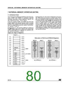
ST90158 - EXTERNAL MEMORY INTERFACE (EXTMI)
7.2 EXTERNAL MEMORY SIGNALS
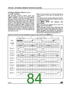
The access to external memory is made using at
least AS, DS, Port 0 and Port 1. RW, DS2, BREQ,
BACK and WAIT signals improve functionality but
are not always present on ST9 devices.
under processor control by setting the HIMP bit
(MODER.0, R235). Under Reset status, DS is held
high with an internal weak pull-up.
The behavior of this signal is affected by the MC,
DS2EN, and BSZ bits in the EMR1 register. Refer
to the Register description.
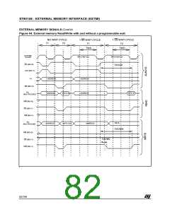
Refer to Figure 44
7.2.1 AS: Address Strobe
AS (Output, Active low, Tristate) is active during
the System Clock high-level phase of each T1
memory cycle: an AS rising edge indicates that
Memory Address and Read/Write Memory control
signals are valid. AS is released in high-imped-
ance during the bus acknowledge cycle or under
the processor control by setting the HIMP bit
(MODER.0, R235). Depending on the device AS is
available as Alternate Function or as a dedicated
pin.
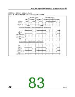
7.2.3 DS2: Data Strobe 2
This additional Data Strobe pin (Alternate Function
Output, Active low, Tristate) is available on some
ST9 devices only. It allows two external memories
to be connected to the ST9, the upper memory
block (A21=1 typically RAM) and the lower memo-
ry block (A21=0 typically ROM) without any exter-
nal logic. The selection between the upper and
lower memory blocks depends on the A21 address
pin value.
Under Reset, AS is held high with an internal weak
pull-up.
The upper memory block is controlled by the DS
pin while the lower memory block is controlled by
the DS2 pin. When the internal memory is ad-
dressed, DS2 is kept high during the whole mem-
ory cycle. DS2 is released in high-impedance dur-
ing bus acknowledge cycle or under processor
control by setting the HIMP bit (MODER.0, R235).
DS2 is enabled via software as the Alternate Func-
tion output of the associated I/O port bit (refer to
specific ST9 version to identify the specific port
and pin).
The behavior of this signal is affected by the MC,
ASAF, ETO, BSZ, LAS[1:0] and UAS[1:0] bits in
the EMR1 or EMR2 registers. Refer to the Regis-
ter description.
7.2.2 DS: Data Strobe
DS (Output, Active low, Tristate) is active during the
internal clock high-level phase of each T2 memory
cycle. During an external memory read cycle, the
data on Port 0 must be valid before the DS rising
edge. During an external memory write cycle, the
data on Port 0 are output on the falling edge of DS
and they are valid on the rising edge of DS. When
the internal memory is accessed DS is kept high
during the whole memory cycle. DS is released in
high-impedance during bus acknowledge cycle or
The behavior of this signal is affected by the
DS2EN, and BSZ bits in the EMR1 register. Refer
to the Register description.
81/199
9

 ETC [ ETC ]