ST90158 - EXTERNAL MEMORY INTERFACE (EXTMI)
7 EXTERNAL MEMORY INTERFACE (EXTMI)
7.1 INTRODUCTION
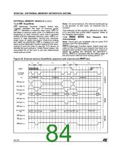
The ST9 External Memory Interface uses two reg-
isters (EMR1 and EMR2) to configure external
memory accesses. Some interface signals are
also affected by WCR - R252 Page 0.
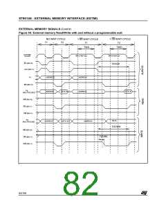
During phase T2, two forms of behavior are possi-
ble. If the memory access is a Read cycle, Port 0
pins are released in high-impedance until the next
T1 phase and the data signals are sampled by the
ST9 on the rising edge of DS. If the memory ac-
cess is a Write cycle, on the falling edge of DS,
Port 0 outputs data to be written in the external
memory. Those data signals are valid on the rising
edge of DS and are maintained stable until the
next address is output. Note that DS is pulled low
at the beginning of phase T2 only during an exter-
nal memory access.
If the two registers EMR1 and EMR2 are set to the
proper values, the memory access cycle is similar
to that of the original ST9, with the only exception
that it is composed of just two system clock phas-
es, named T1 and T2.
During phase T1, the memory address is output on
the AS falling edge and is valid on the rising edge
of AS. Port0 and Port 1 maintain the address sta-
ble until the following T1 phase.
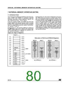
Figure 43. Page 21 Registers
n
Page 21
FFh
FEh
FDh
FCh
FBh
FAh
F9h
F8h
F7h
F6h
F5h
F4h
F3h
F2h
F1h
F0h
R255
R254
R253
R252
R251
R250
R249
R248
R247
R246
R245
R244
R243
R242
R241
R240
Relocation of P[3:0] and DPR[3:0] Registers
SSPL
SSPL
SSPH
USPL
USPH
MODER
PPR
RP1
RP0
FLAGR
CICR
P5
SSPH
USPL
USPH
MODER
PPR
RP1
RP0
FLAGR
CICR
P5
DMASR
ISR
DMASR
ISR
DMASR
ISR
MMU
EMR2
EMR1
CSR
EMR2
EMR1
CSR
P3
P2
P1
P4
P4
EMR2
EMR1
CSR
P3
P2
P1
P0
DPR3
DPR2
DPR1
DPR0
DPR3
DPR2
DPR1
DPR0
EXT.MEM
P0
DPR3
DPR2
DPR1
DPR0
Bit DPRREM=0
Bit DPRREM=1
MMU
80/199
9

 ETC [ ETC ]