ST90158 - EXTERNAL MEMORY INTERFACE (EXTMI)
REGISTER DESCRIPTION (Cont’d)
Bit 1:0 = UAS[1:0]: Upper memory address strobe
stretch.
tional wait cycles. UDS = 7 adds the maximum 7
INTCLK cycles (reset condition).
These two bits contain the number of wait cycles
(from 0 to 3) to add to the System Clock to stretch
AS during external upper memory block accesses
(MSB of 22-bit internal address=1). The reset val-
ue is 3.
Bit 2:0 = LDS[2:0]: Lower memory data strobe
stretch.
These bits contain the number of INTCLK cycles
to be added automatically to DS or DS2 (depend-
ing on the DS2EN bit of the EMR1 register) for ex-
ternal lower memory block accesses. LDS = 0
adds no additional wait cycles, LDS = 7 adds the
maximum 7 INTCLK cycles (reset condition).
WARNING: The EMR2 register cannot be written
during an interrupt service routine.
WAIT CONTROL REGISTER (WCR)
R252 - Read/Write
Register Page: 0
Note 1: The number of clock cycles added refers
to INTCLK and NOT to CPUCLK.
Note 2: The distinction between the Upper memo-
ry block and the Lower memory block allows differ-
ent wait cycles between the first 2 Mbytes and the
second 2 Mbytes, and allows 2 different data
strobe signals to be used to access 2 different
memories.
Reset Value: 0111 1111 (7Fh)
7
0
0
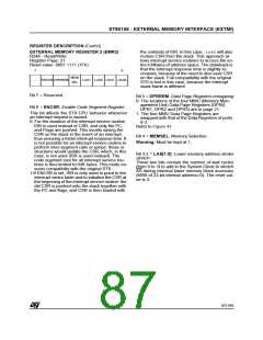
WDGEN UDS2 UDS1 UDS0 LDS2 LDS1 LDS0
Typically, the RAM will be located above address
0x200000 and the ROM below address
0x1FFFFF, with different access times. No extra
hardware is required as DS is used to access the
upper memory block and DS2 is used to access
the lower memory block.
Bit 7 = Reserved, forced by hardware to 0.
Bit 6 = WDGEN: Watchdog Enable.
For a description of this bit, refer to the Timer/
Watchdog chapter.
WARNING: Clearing this bit has the effect of set-
ting the Timer/Watchdog to Watchdog mode. Un-
less this is desired, it must be set to “1”.
WARNING: The reset value of the Wait Control
Register gives the maximum number of Wait cy-
cles for external memory. To get optimum perfor-
mance from the ST9, the user should write the
UDS[2:0] and LDS[2:0] bits to 0, if the external ad-
dressed memories are fast enough.
Bit 5:3 = UDS[2:0]: Upper memory data strobe
stretch.
These bits contain the number of INTCLK cycles
to be added automatically to DS for external upper
memory block accesses. UDS = 0 adds no addi-
88/199
9

 ETC [ ETC ]