ST90158 - EXTERNAL MEMORY INTERFACE (EXTMI)
7.3 REGISTER DESCRIPTION
EXTERNAL MEMORY REGISTER 1 (EMR1)
R245 - Read/Write
Register Page: 21
Bit 4 = ASAF: Address Strobe as Alternate Func-
tion.
Depending on the device, AS can be either a ded-
icated pin or a port Alternate Function. This bit is
used only in this last case.
Reset value: 1000 0000 (80h)
0: AS Alternate function disabled.
1: AS Alternate Function enabled.
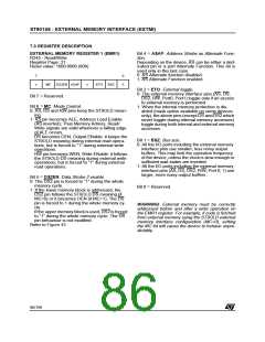
7
0
x
MC
DS2EN ASAF
x
ETO
BSZ
X
Bit 2 = ETO: External toggle.
0: The external memory interface pins (AS, DS,
DS2, RW, Port0, Port1) toggle only if an access
to external memory is performed.
1: When the internal memory protection is dis-
abled (mask option available on some devices
only), the above pins (except DS and DS2 which
never toggle during internal memory accesses)
toggle during both internal and external memory
accesses.
Bit 7 = Reserved.
Bit 6 = MC: Mode Control.
0: AS, DS and RW pins keep the ST9OLD mean-
ing.
1: AS pin becomes ALE, Address Load Enable
(AS inverted); Thus Memory Adress, Read/
Write signals are valid whenever a falling edge
of ALE occurs.
DS becomes OEN, Output ENable: it keeps the
ST9OLD meaning during external read opera-
tions, but is forced to “1” during external write
operations.
RW pin becomes WEN, Write ENable: it follows
the ST9OLD DS meaning during external write
operations, but is forced to “1” during external
read operations.
Bit 1 = BSZ: Bus size.
0: All the I/O ports including the external memory
interface pins use smaller, less noisy output
buffers. This may limit the operation frequency
of the device, unless the clock is slow enough or
sufficient wait states are inserted.
1: All the I/O ports including the external memory
interface pins (AS, DS, DS2, R/W, Port 0, 1) use
larger, more noisy output buffers .
Bit 5 = DS2EN: Data Strobe 2 enable.
0: The DS2 pin is forced to “1” during the whole
memory cycle.
1: If the lower memory block is addressed, the
DS2 pin follows the ST9OLD DS meaning (if
MC=0) or it becomes OEN (if MC=1). The DS
pin is forced to 1 during the whole memory cy-
cle.
Bit 0 = Reserved.
WARNING: External memory must be correctly
addressed before and after a write operation on
the EMR1 register. For example, if code is fetched
from external memory using the ST9OLD external
memory interface configuration (MC=0), setting
the MC bit will cause the device to behave unpre-
dictably.
If the upper memory block is used, DS2 is forced
to “1” during the whole memory cycle. The DS
pin behaviour is not modified.
Refer to Figure 45
86/199
9

 ETC [ ETC ]