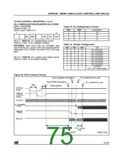
ST90158 - RESET AND CLOCK CONTROL UNIT (RCCU)
RESET/STOP MANAGER (Cont’d)
The on-chip Timer/Watchdog generates a reset
condition if the Watchdog mode is enabled
(WCR.WDEN cleared, R252 page 0), and if the
programmed period elapses without the specific
code (AAh, 55h) written to the appropriate register.
The input pin RESET is not driven low by the on-
chip reset generated by the Timer/Watchdog.
At the end of the Boot routine the Program Coun-
ter will be set to the location specified in the Reset
Vector located in the lowest two bytes of memory.
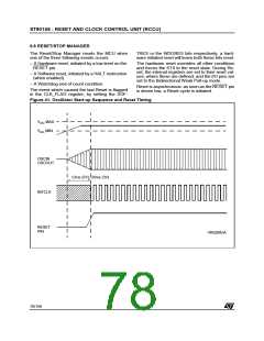
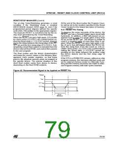
6.6.1 RESET Pin Timing
To improve the noise immunity of the device, the
RESET pin has a Schmitt trigger input circuit with
hysteresis. In addition, a filter will prevent an un-
wanted reset in case of a single glitch of less than
50 ns on the RESET pin. The device is certain to
reset if a negative pulse of more than 20µs is ap-
plied. When the RESET pin goes high again, a de-
lay of up to 4µs will elapse before the RCCU de-
tects this rising front. From this event on, 510 os-
cillator clock cycles (CLOCK1) are counted before
exiting the Reset state (+-1CLOCK1 period de-
pending on the delay between the positive edge
the RCCU detects and the first rising edge of
CLOCK1)
When the RESET pin goes high again, 510 oscilla-
tor clock cycles (CLOCK1) are counted before ex-
iting the Reset state (+-1 CLOCK1 period, depend-
ing on the delay between the rising edge of the RE-
SET pin and the first rising edge of CLOCK1). Sub-
sequently a short Boot routine is executed from the
device internal Boot ROM, and control then passes
to the user program.
The Boot routine sets the device characteristics
and loads the correct values in the Memory Man-
agement Unit’s pointer registers, so that these
point to the physical memory areas as mapped in
the specific device. The precise duration of this
short Boot routine varies from device to device,
depending on the Boot ROM contents.
If the ST9 is a ROMLESS version, without on-chip
program memory, the mermory interface ports are
set to external memory mode (i.e Alternate Func-
tion) and the memory accesses are made to exter-
nal Program memory with wait cycles insertion.
Figure 42. Recommended Signal to be Applied on RESET Pin
V
RESET
V
DD
0.7 V
DD
0.3 V
DD
20 µs
Minimum
79/199
9

 ETC [ ETC ]