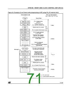
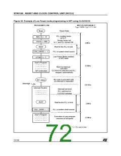
ST90158 - RESET AND CLOCK CONTROL UNIT (RCCU)
CLOCK CONTROL REGISTERS (Cont’d)
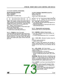
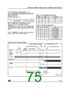
PLL CONFIGURATION REGISTER (PLLCONF)
R246 - Read/Write
Register Page: 55
Table 13. PLL Multiplication Factors
MX1
MX0
CLOCK2 x
Reset Value: xx00 x111
1
0
1
0
0
0
1
1
14
10
8
7
0
-
-
MX1 MX0
-
DX2 DX1 DX0
6
Bit 5:4 = MX[1:0]: PLL Multiplication Factor.
Refer to Table 13 for multiplier settings.
Table 14. Divider Configuration
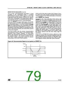
WARNING: After these bits are modified, take
care that the PLL lock-in time has elapsed before
setting the CSU_CKSEL bit in the CLK_FLAG reg-
ister.
DX2
0
DX1
0
DX0
0
CK
PLL CLOCK/1
PLL CLOCK/2
PLL CLOCK/3
PLL CLOCK/4
PLL CLOCK/5
PLL CLOCK/6
PLL CLOCK/7
0
0
1
0
1
0
0
1
1
Bit 2:0 = DX[2:0]: PLL output clock divider factor.
Refer to Table 14 for divider settings.
1
0
0
1
0
1
1
1
0
CLOCK2
(PLL OFF, Reset State)
1
1
1
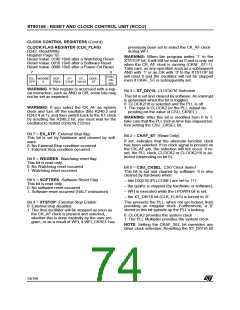
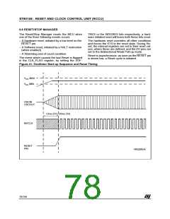
Figure 36. RCCU General Timing
User program execution
Boot ROM execution
PLL switched on by user
PLL selected by user
20µs
< 4µs
Reset phase
External
Reset
Filtered
External
Reset
CLOCK2
PLL Multiplier
clock
Internal
Reset
INTCLK
510 x CLOCK1
PLL
Lock-in
time
Exit from RESET
VR02113B
75/199
9

 ETC [ ETC ]