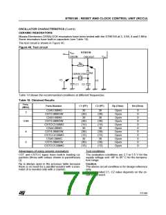
ST90158 - RESET AND CLOCK CONTROL UNIT (RCCU)
6.4 CLOCK CONTROL REGISTERS
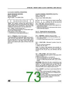
MODE REGISTER (MODER)
R235 - Read/Write
System Register
CLOCK CONTROL REGISTER (CLKCTL)
R240 - Read Write
Register Page: 55
Reset Value: 1110 0000 (E0h)
Reset Value: 0000 0000 (00h)
0
7
7
0
INT_S
EL
SRE- CKAF_S WFI_CKS LPOW
-
-
DIV2 PRS2 PRS1 PRS0
-
-
-
-
-
SEN
EL
EL
FI
*Note: This register contains bits which relate to
other functions; these are described in the chapter
dealing with Device Architecture. Only those bits
relating to Clock functions are described here.
Bit 7 = INT_SEL: Interrupt Selection.
0: The external interrupt channel input signal is se-
lected (Reset state)
1: Select the internal RCCU interrupt as the source
of the interrupt request
Bit 5 = DIV2: OSCIN Divided by 2.
This bit controls the divide by 2 circuit which oper-
ates on the OSCIN Clock.
0: No division of the OSCIN Clock
1: OSCIN clock is internally divided by 2
Bit 4:6 = Reserved for test purposes
Must be kept reset for normal operation.
Bit 3 = SRESEN: Software Reset Enable.
0: The HALT instruction turns off the quartz, the
PLL and the CCU
Bit 4:2 = PRS[2:0]: Clock Prescaling.
These bits define the prescaler value used to pres-
cale CPUCLK from INTCLK. When these three
bits are reset, the CPUCLK is not prescaled, and is
equal to INTCLK; in all other cases, the internal
clock is prescaled by the value of these three bits
plus one.
1: A Reset is generated when HALT is executed
Bit 2 = CKAF_SEL: Alternate Function Clock Se-
lect.
0: CK_AF clock not selected
1: Select CK_AF clock
Note: To check if the selection has actually oc-
curred, check that CKAF_ST is set. If no clock is
present on the CK_AF pin, the selection will not
occur.
Bit 1 = WFI_CKSEL: WFI Clock Select.
This bit selects the clock used in Low power WFI
mode if LPOWFI = 1.
0: INTCLK during WFI is CLOCK2/16
1: INTCLK during WFI is CK_AF, providing it is
present. In effect this bit sets CKAF_SEL in WFI
mode
WARNING: When the CK_AF is selected as Low
Power WFI clock but the XTAL is not turned off
(R242.4 = 0), after exiting from the WFI, CK_AF
will be still selected as system clock. In this case,
reset the R240.2 bit to switch back to the XT.
Bit 0 = LPOWFI: Low Power mode during Wait For
Interrupt.
0: Low Power mode during WFI disabled. When
WFI is executed, the CPUCLK is stopped and
INTCLK is unchanged
1: The ST9 enters Low Power mode when the WFI
instruction is executed. The clock during this
state depends on WFI_CKSEL
73/199
9

 ETC [ ETC ]