ST90158 - MULTIFUNCTION TIMER (MFT)
MULTIFUNCTION TIMER (Cont’d)
INTERRUPT/DMA MASK REGISTER (IDMR)
R255 - Read/Write
Register Page: 10
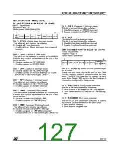
Bit 1 = CM1I: Compare 1 Interrupt mask.
This bit is set and cleared by software.
0: Disable compare on CMP1R interrupt
1: Enable compare on CMP1R interrupt
Reset value: 0000 0000 (00h)
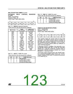
7
0
GT-
IEN
CM0
D
CP0D CP0I CP1I
CM0I CM1I OUI
Bit 0 = OUI:
Overflow/Underflow interrupt mask.
This bit is set and cleared by software.
0: Disable Overflow/Underflow interrupt
1: Enable Overflow/Underflow interrupt
Bit 7 = GTIEN: Global timer interrupt enable.
This bit is set and cleared by software.
0: Disable all Timer interrupts
1: Enable all timer Timer Interrupts from enabled
sources
DMA COUNTER POINTER REGISTER (DCPR)
R240 - Read/Write
Register Page: 9
Reset value: undefined
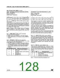
Bit 6 = CP0D: Capture 0 DMA mask.
This bit is set by software to enable a Capt0 DMA
transfer and cleared by hardware at the end of the
block transfer.
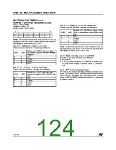
7
0
DMA REG/
SRCE MEM
0: Disable capture on REG0R DMA
1: Enable capture on REG0R DMA
DCP7 DCP6 DCP5 DCP4 DCP3 DCP2
Bits 7:2 = DCP[7:2]: MSBs of DMA counter regis-
ter address.
These are the most significant bits of the DMA
counter register address programmable by soft-
ware. The DCP2 bit may also be toggled by hard-
ware if the Timer DMA section for the Compare 0
channel is configured in Swap mode.
Bit 5 = CP0I: Capture 0 interrupt mask.
0: Disable capture on REG0R interrupt
1: Enable capture on REG0R interrupt (or Capt0
DMA End of Block interrupt if CP0D=1)
Bit 4 = CP1I: Capture 1 interrupt mask.
This bit is set and cleared by software.
0: Disable capture on REG1R interrupt
1: Enable capture on REG1R interrupt
Bit 1 = DMA-SRCE: DMA source selection.
This bit is set and cleared by hardware.
0: DMA source is a Capture on REG0R register
1: DMA destination is a Compare on CMP0R reg-
ister
Bit 3 = CM0D: Compare 0 DMA mask.
This bit is set by software to enable a Comp0 DMA
transfer and cleared by hardware at the end of the
block transfer.
0: Disable compare on CMP0R DMA
1: Enable compare on CMP0R DMA
Bit 0 = REG/MEM: DMA area selection.
This bit is set and cleared by software. It selects
the source and destination of the DMA area
0: DMA from/to memory
Bit 2 = CM0I: Compare 0 Interrupt mask.
This bit is set and cleared by software.
0: Disable compare on CMP0R interrupt
1: Enable compare on CMP0R interrupt (or
Comp0 DMA End of Block interrupt if CM0D=1)
1: DMA from/to Register File
127/199
9

 ETC [ ETC ]