ST90158 - MULTIFUNCTION TIMER (MFT)
MULTIFUNCTION TIMER (Cont’d)
INTERRUPT/DMA CONTROL REGISTER
(IDCR)
R243 - Read/Write
Register Page: 9
Reset value: 1100 0111 (C7h)
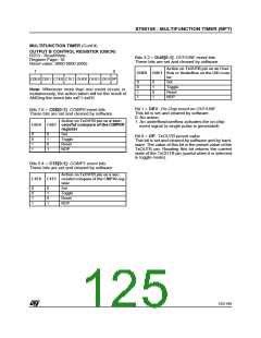
Bit 3 = SWEN: Swap function enable.
This bit is set and cleared by software.
0: Disable Swap mode
1: Enable Swap mode for both DMA channels.
7
0
DCT SWE
Bits 2:0 = PL[2:0]: Interrupt/DMA priority level.
With these three bits it is possible to select the In-
terrupt and DMA priority level of each timer, as one
of eight levels (see Interrupt/DMA chapter).
CPE CME DCTS
PL2 PL1 PL0
D
N
Bit 7 = CPE: Capture 0 EOB.
This bit is set by hardware when the End Of Block
condition is reached during a Capture 0 DMA op-
eration with the Swap mode enabled. When Swap
mode is disabled (SWEN bit = “0”), the CPE bit is
forced to 1 by hardware.
0: No end of block condition
1: Capture 0 End of block
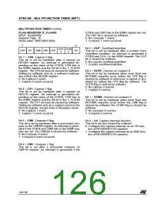
I/O CONNECTION REGISTER (IOCR)
R248 - Read/Write
Register Page: 9
Reset value: 1111 1100 (FCh)
7
0
SC1 SC0
Bit 6 = CME: Compare 0 EOB.
This bit is set by hardware when the End Of Block
condition is reached during a Compare 0 DMA op-
eration with the Swap mode enabled. When the
Swap mode is disabled (SWEN bit = “0”), the CME
bit is forced to 1 by hardware.
0: No end of block condition
1: Compare 0 End of block
Bits 7:2 = not used.
Bit 1 = SC1: Select connection odd.
This bit is set and cleared by software. It selects if
the TxOUTA and TxINA pins for Timer 1 and Timer
3 are connected on-chip or not.
0: T1OUTA / T1INA and T3OUTA/ T3INA uncon-
nected
Bit 5 = DCTS: DMA capture transfer source.
This bit is set and cleared by software. It selects
the source of the DMA operation related to the
channel associated with the Capture 0.
Note: The I/O port source is available only on spe-
cific devices.
1: T1OUTA connected internally to T1INA and
T3OUTA connected internally to T3INA
Bit 0 = SC0: Select connection even.
This bit is set and cleared by software. It selects if
the TxOUTA and TxINA pins for Timer 0 and Timer
2 are connected on-chip or not.
0: T0OUTA / T0INA and T2OUTA/ T2INA uncon-
nected
0: REG0R register
1: I/O port.
Bit 4 = DCTD: DMA compare transfer destination.
This bit is set and cleared by software. It selects
the destination of the DMA operation related to the
channel associated with Compare 0.
Note: The I/O port destination is available only on
specific devices.
1: T0OUTA connected internally to T0INA and
T2OUTA connected internally to T2INA
Note: Timer 1 and 2 are available only on some
devices. Refer to the device block diagram and
register map.
0: CMP0R register
1: I/O port
129/199
9

 ETC [ ETC ]