ST90158 - MULTIFUNCTION TIMER (MFT)
MULTIFUNCTION TIMER (Cont’d)
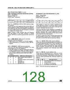
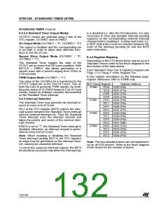
DMA ADDRESS POINTER REGISTER (DAPR)
R241 - Read/Write
Register Page: 9
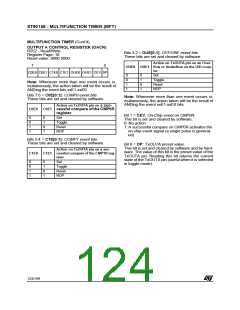
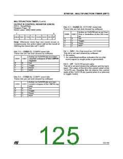
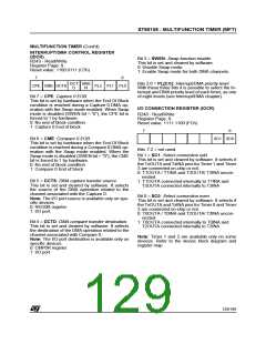
INTERRUPT VECTOR REGISTER (T_IVR)
R242 - Read/Write
Register Page: 9
Reset value: xxxx xxx0
Reset value: undefined
7
0
7
0
0
DAP DAP
7
DMA PRG
SRCE /DAT
DAP5 DAP4 DAP3 DAP2
V4
V3
V2
V1
V0
W1
W0
6
Bits 7:2 = DAP[7:2]: MSB of DMA address regis-
ter location.
These are the most significant bits of the DMA ad-
dress register location programmable by software.
The DAP2 bit may also be toggled by hardware if
the Timer DMA section for the Compare 0 channel
is configured in Swap mode.
This register is used as a vector, pointing to the
16-bit interrupt vectors in memory which contain
the starting addresses of the three interrupt sub-
routines managed by each timer.
Only one Interrupt Vector Register is available for
each timer, and it is able to manage three interrupt
groups, because the 3 least significant bits are
fixed by hardware depending on the group which
generated the interrupt request.
Note: During a DMA transfer with the Register
File, the DAPR is not used; however, in Swap
mode, DAPR(2) is used to point to the correct ta-
ble.
In order to determine which request generated the
interrupt within a group, the T_FLAGR register can
be used to check the relevant interrupt source.
Bit 1 = DMA-SRCE: DMA source selection.
This bit is fixed by hardware.
0: DMA source is a Capture on REG0R register
1: DMA destination is a Compare on the CMP0R
register
Bits 7:3 = V[4:0]: MSB of the vector address.
These bits are user programmable and contain the
five most significant bits of the Timer interrupt vec-
tor addresses in memory. In any case, an 8-bit ad-
dress can be used to indicate the Timer interrupt
vector locations, because they are within the first
256 memory locations (see Interrupt and DMA
chapters).
Bit 0 = PRG/DAT: DMA memory selection.
This bit is set and cleared by software. It is only
meaningful if DCPR.REG/MEM=0.
0: The ISR register is used to extend the address
of data transferred by DMA (see MMU chapter).
1: The DMASR register is used to extend the ad-
dress of data transferred by DMA (see MMU
chapter).
Bits 2:1 = W[1:0]: Vector address bits.
These bits are equivalent to bit 1 and bit 2 of the
Timer interrupt vector addresses in memory. They
are fixed by hardware, depending on the group of
sources which generated the interrupt request as
follows:.
REG/MEM PRG/DAT
DMA Source/Destination
0
0
ISR register used to address
memory
W1
W0
Interrupt Source
0
1
DMASR register used to address
memory
Register file
0
0
1
1
0
1
0
1
Overflow/Underflow even interrupt
Not available
Capture event interrupt
Compare event interrupt
1
1
0
1
Register file
Bit 0 = This bit is forced by hardware to 0.
128/199
9

 ETC [ ETC ]