ST72104G, ST72215G, ST72216G, ST72254G
8-BIT A/D CONVERTER (ADC) (Cont’d)
12.5.3.2 Digital A/D Conversion Result
The analog input ports must be configured as in-
put, no pull-up, no interrupt. Refer to the «I/O
ports» chapter. Using these pins as analog inputs
does not affect the ability of the port to be read as
a logic input.
The conversion is monotonic, meaning that the re-
sult never decreases if the analog input does not
and never increases if the analog input does not.
If the input voltage (V ) is greater than or equal
AIN
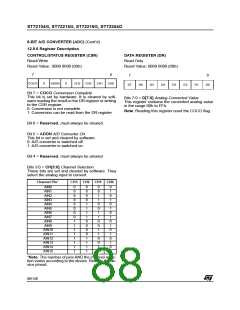
In the CSR register:
to V
(high-level voltage reference) then the
DDA
conversion result in the DR register is FFh (full
scale) without overflow indication.
– Select the CH[3:0] bits to assign the analog
channel to be converted.
ADC Conversion
If input voltage (V ) is lower than or equal to
AIN
V
(low-level voltage reference) then the con-
version result in the DR register is 00h.
SSA
In the CSR register:
– Set the ADON bit to enable the A/D converter
and to start the first conversion. From this time
on, the ADC performs a continuous conver-
sion of the selected channel.
The A/D converter is linear and the digital result of
the conversion is stored in the ADCDR register.
The accuracy of the conversion is described in the
parametric section.
When a conversion is complete
R
is the maximum recommended impedance
– The COCO bit is set by hardware.
– No interrupt is generated.
– The result is in the DR register and remains
valid until the next conversion has ended.
AIN
for an analog input signal. If the impedance is too
high, this will result in a loss of accuracy due to
leakage and sampling not being completed in the
alloted time.
A write to the CSR register (with ADON set) aborts
the current conversion, resets the COCO bit and
starts a new conversion.
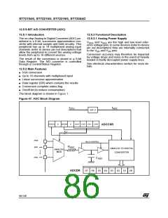
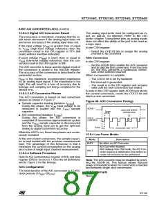
12.5.3.3 A/D Conversion Phases
The A/D conversion is based on two conversion
phases as shown in Figure 2:
Figure 48. ADC Conversion Timings
■ Sample capacitor loading [duration: t
]
LOAD
During this phase, the V
input voltage to be
AIN
ADON
measured is loaded into the C
capacitor.
sample
ADC
ADCCSR WRITE
OPERATION
t
CONV
■ A/D conversion [duration: t
]
CONV
During this phase, the A/D conversion is
computed (8 successive approximations cycles)
HOLD
CONTROL
and the C
sample capacitor is disconnected
ADC
from the analog input pin to get the optimum
analog to digital conversion accuracy.
t
LOAD
COCO BIT SET
While the ADC is on, these two phases are contin-
uously repeated.
12.5.4 Low Power Modes
At the end of each conversion, the sample capaci-
tor is kept loaded with the previous measurement
load. The advantage of this behaviour is that it
minimizes the current consumption on the analog
pin in case of single input channel measurement.
Mode
WAIT
Description
No effect on A/D Converter
A/D Converter disabled.
After wakeup from Halt mode, the A/D Con-
verter requires a stabilisation time before ac-
curate conversions can be performed.
HALT
12.5.3.4 Software Procedure
Refer to the control/status register (CSR) and data
register (DR) in Section 0.1.6 for the bit definitions
and to Figure 2 for the timings.
Note: The A/D converter may be disabled by reset-
ting the ADON bit. This feature allows reduced
power consumption when no conversion is needed
and between single shot conversions.
ADC Configuration
The total duration of the A/D conversion is 12 ADC
12.5.5 Interrupts
clock periods (1/f
=2/f
).
ADC
CPU
None
87/140

 ETC [ ETC ]