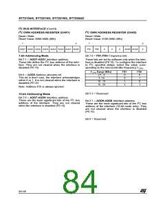
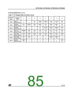
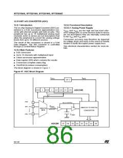
ST72104G, ST72215G, ST72216G, ST72254G
2
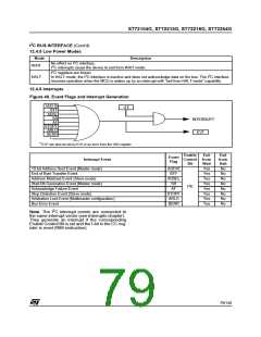
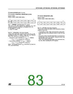
I C BUS INTERFACE (Cont’d)
2
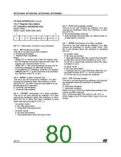
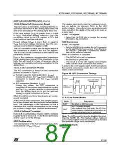
I C CLOCK CONTROL REGISTER (CCR)
2
Read / Write
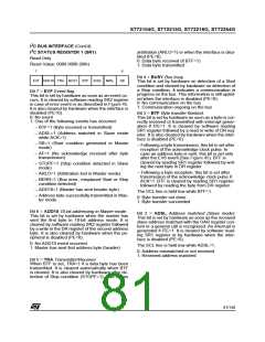
I C DATA REGISTER (DR)
Reset Value: 0000 0000 (00h)
Read / Write
Reset Value: 0000 0000 (00h)
7
0
7
0
FM/SM CC6
CC5
CC4
CC3
CC2
CC1
CC0
D7
D6
D5
D4
D3
D2
D1
D0
2
Bit 7 = FM/SM Fast/Standard I C mode.
This bit is set and cleared by software. It is not
cleared when the interface is disabled (PE=0).
2
Bit 7:0 = D7-D0 8-bit Data Register.
These bits contain the byte to be received or trans-
mitted on the bus.
0: Standard I C mode
2
1: Fast I C mode
– Transmitter mode: Byte transmission start auto-
matically when the software writes in the DR reg-
ister.
Bit 6:0 = CC6-CC0 7-bit clock divider.
These bits select the speed of the bus (F
) de-
SCL
2
pending on the I C mode. They are not cleared
when the interface is disabled (PE=0).
– Receiver mode: the first data byte is received au-
tomatically in the DR register using the least sig-
nificant bit of the address.
– Standard mode (FM/SM=0): F
<= 100kHz
SCL
F
= F
/(2x([CC6..CC0]+2))
CPU
Then, the following data bytes are received one
by one after reading the DR register.
SCL
– Fast mode (FM/SM=1): F
> 100kHz
SCL
F
= F
/(3x([CC6..CC0]+2))
CPU
SCL
Note: The programmed F
SCL and SDA lines.
assumes no load on
SCL
83/140

 ETC [ ETC ]