ST72104G, ST72215G, ST72216G, ST72254G
2
I C BUS INTERFACE (Cont’d)
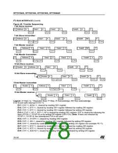
12.4.7 Register Description
2
Bit 2 = ACK Acknowledge enable.
This bit is set and cleared by software. It is also
cleared by hardware when the interface is disa-
bled (PE=0).
0: No acknowledge returned
1: Acknowledge returned after an address byte or
a data byte is received
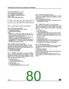
I C CONTROL REGISTER (CR)
Read / Write
Reset Value: 0000 0000 (00h)
7
0
0
0
PE
ENGC START ACK STOP
ITE
Bit 1 = STOP Generation of a Stop condition.
This bit is set and cleared by software. It is also
cleared by hardware in master mode. Note: This
bit is not cleared when the interface is disabled
(PE=0).
Bit 7:6 = Reserved. Forced to 0 by hardware.
Bit 5 = PE Peripheral enable.
This bit is set and cleared by software.
0: Peripheral disabled
1: Master/Slave capability
Notes:
– When PE=0, all the bits of the CR register and
the SR register except the Stop bit are reset. All
outputs are released while PE=0
– In master mode:
0: No stop generation
1: Stop generation after the current byte transfer
or after the current Start condition is sent. The
STOP bit is cleared by hardware when the Stop
condition is sent.
– When PE=1, the corresponding I/O pins are se-
– In slave mode:
0: No stop generation
1: Release the SCL and SDA lines after the cur-
rent byte transfer (BTF=1). In this mode the
STOP bit has to be cleared by software.
lected by hardware as alternate functions.
2
– To enable the I C interface, write the CR register
TWICE with PE=1 as the first write only activates
the interface (only PE is set).
Bit 4 = ENGC Enable General Call.
This bit is set and cleared by software. It is also
cleared by hardware when the interface is disa-
bled (PE=0). The 00h General Call address is ac-
knowledged (01h ignored).
0: General Call disabled
1: General Call enabled
Bit 0 = ITE Interrupt enable.
This bit is set and cleared by software and cleared
by hardware when the interface is disabled
(PE=0).
0: Interrupts disabled
1: Interrupts enabled
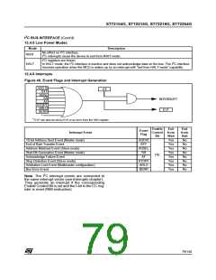
Refer to Figure 46 for the relationship between the
events and the interrupt.
SCL is held low when the ADD10, SB, BTF or
ADSL flags or an EV6 event (See Figure 45) is de-
tected.
Bit 3 = START Generation of a Start condition.
This bit is set and cleared by software. It is also
cleared by hardware when the interface is disa-
bled (PE=0) or when the Start condition is sent
(with interrupt generation if ITE=1).
– In master mode:
0: No start generation
1: Repeated start generation
– In slave mode:
0: No start generation
1: Start generation when the bus is free
80/140

 ETC [ ETC ]