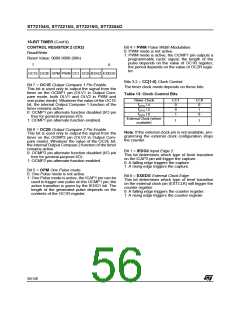
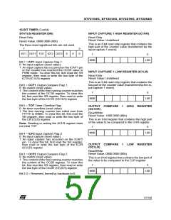
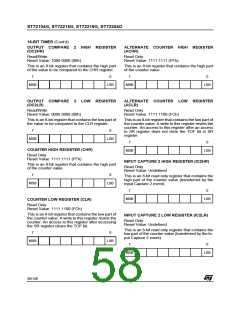
ST72104G, ST72215G, ST72216G, ST72254G
12.3 SERIAL PERIPHERAL INTERFACE (SPI)
12.3.1 Introduction
12.3.3 General description
The Serial Peripheral Interface (SPI) allows full-
duplex, synchronous, serial communication with
external devices. An SPI system may consist of a
master and one or more slaves or a system in
which devices may be either masters or slaves.
The SPI is connected to external devices through
4 alternate pins:
– MISO: Master In Slave Out pin
– MOSI: Master Out Slave In pin
– SCK: Serial Clock pin
The SPI is normally used for communication be-
tween the microcontroller and external peripherals
or another microcontroller.
– SS: Slave select pin
Refer to the Pin Description chapter for the device-
specific pin-out.
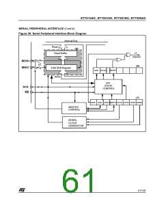
A basic example of interconnections between a
single master and a single slave is illustrated on
Figure 37.
12.3.2 Main Features
The MOSI pins are connected together as are
MISO pins. In this way data is transferred serially
between master and slave (most significant bit
first).
■ Full duplex, three-wire synchronous transfers
■ Master or slave operation
■ Four master mode frequencies
■ Maximum slave mode frequency = fCPU/2.
■ Four programmable master bit rates
■ Programmable clock polarity and phase
■ End of transfer interrupt flag
When the master device transmits data to a slave
device via MOSI pin, the slave device responds by
sending data to the master device via the MISO
pin. This implies full duplex transmission with both
data out and data in synchronized with the same
clock signal (which is provided by the master de-
vice via the SCK pin).
■ Write collision flag protection
■ Master mode fault protection capability.
Thus, the byte transmitted is replaced by the byte
received and eliminates the need for separate
transmit-empty and receiver-full bits. A status flag
is used to indicate that the I/O operation is com-
plete.
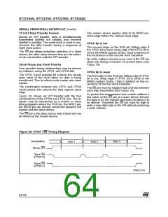
Four possible data/clock timing relationships may
be chosen (see Figure 40) but master and slave
must be programmed with the same timing mode.
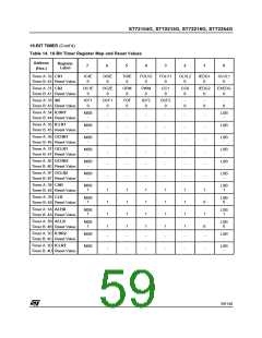
Figure 37. Serial Peripheral Interface Master/Slave
MASTER
SLAVE
MSBit
LSBit
MSBit
LSBit
MISO
MOSI
MISO
MOSI
8-BIT SHIFT REGISTER
8-BIT SHIFT REGISTER
SPI
CLOCK
SCK
SCK
GENERATOR
SS
SS
+5V
60/140

 ETC [ ETC ]