ST72104G, ST72215G, ST72216G, ST72254G
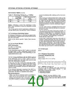
11 MISCELLANEOUS REGISTERS
The miscellaneous registers allow control over
several different features such as the external in-
terrupts or the I/O alternate functions.
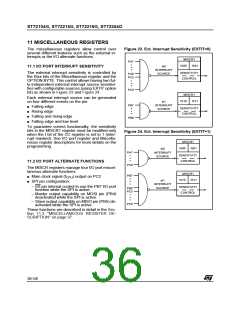
Figure 23. Ext. Interrupt Sensitivity (EXTIT=0)
MISCR1
IS00 IS01
PA7
ei0
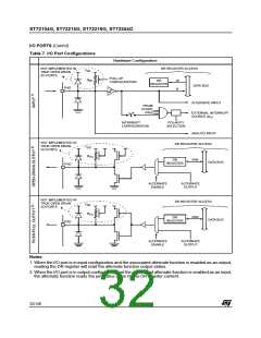
11.1 I/O PORT INTERRUPT SENSITIVITY
INTERRUPT
SOURCE
The external interrupt sensitivity is controlled by
the ISxx bits of the Miscellaneous register and the
OPTION BYTE. This control allows having two ful-
ly independent external interrupt source sensitivi-
ties with configurable sources (using EXTIT option
bit) as shown in Figure 23 and Figure 24.
SENSITIVITY
CONTROL
PA0
PC5
PC0
MISCR1
Each external interrupt source can be generated
on four different events on the pin:
IS10
IS11
ei1
PB7
PB0
INTERRUPT
SOURCE
■ Falling edge
SENSITIVITY
CONTROL
■ Rising edge
■ Falling and rising edge
■ Falling edge and low level
To guarantee correct functionality, the sensitivity
bits in the MISCR1 register must be modified only
when the I bit of the CC register is set to 1 (inter-
rupt masked). See I/O port register and Miscella-
neous register descriptions for more details on the
programming.
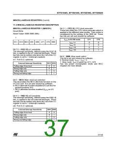
Figure 24. Ext. Interrupt Sensitivity (EXTIT=1)
MISCR1
IS00
IS01
ei0
PA7
INTERRUPT
SOURCE
SENSITIVITY
CONTROL
11.2 I/O PORT ALTERNATE FUNCTIONS
PA0
PB7
The MISCR registers manage four I/O port miscel-
laneous alternate functions:
MISCR1
■ Main clock signal (f
) output on PC2
CPU
IS10
IS11
ei1
■ SPI pin configuration:
INTERRUPT
SOURCE
– SS pin internal control to use the PB7 I/O port
function while the SPI is active.
– Master output capability on MOSI pin (PB4)
deactivated while the SPI is active.
SENSITIVITY
CONTROL
PB0
PC5
– Slave output capability on MISO pin (PB5) de-
activated while the SPI is active.
PC0
These functions are described in detail in the Sec-
tion 11.3 "MISCELLANEOUS REGISTER DE-
SCRIPTION" on page 37.
36/140

 ETC [ ETC ]