ST72104G, ST72215G, ST72216G, ST72254G
MISCELLANEOUS REGISTERS (Cont’d)
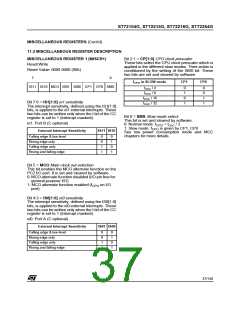
MISCELLANEOUS REGISTER 2 (MISCR2)
Read/Write
Reset Value: 0000 0000 (00h)
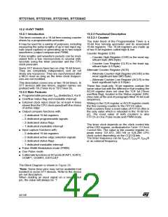
7
0
0
0
0
0
MOD SOD SSM SSI
Bit 7:4 = Reserved always read as 0
Bit 3 = MOD SPI Master Output Disable
This bit is set and cleared by software. When set, it
disables the SPI Master (MOSI) output signal.
0: SPI Master Output enabled.
1: SPI Master Output disabled.
Bit 2 = SOD SPI Slave Output Disable
This bit is set and cleared by software. When set it
disable the SPI Slave (MISO) output signal.
0: SPI Slave Output enabled.
1: SPI Slave Output disabled.
Bit 1 = SSM SS mode selection
This bit is set and cleared by software.
0: Normal mode - the level of the SPI SS signal is
input from the external SS pin.
1: I/O mode, the level of the SPI SS signal is read
from the SSI bit.
Bit 0 = SSI SS internal mode
This bit replaces the SS pin of the SPI when the
SSM bit is set to 1. (see SPI description). It is set
and cleared by software.
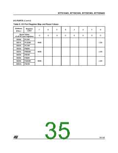
Table 10. Miscellaneous Register Map and Reset Values
Address
(Hex.)
Register
Label
7
6
5
4
3
2
1
0
MISCR1
Reset Value
IS11
0
IS10
0
MCO
0
IS01
0
IS00
0
CP1
0
CP0
0
SMS
0
0020h
0040h
MISCR2
Reset Value
MOD
0
SOD
0
SSM
0
SSI
0
0
0
0
0
38/140

 ETC [ ETC ]