ST72104G, ST72215G, ST72216G, ST72254G
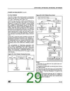
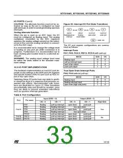
Figure 22. Interrupt I/O Port State Transitions
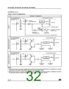
I/O PORTS (Cont’d)
CAUTION: The alternate function must not be ac-
tivated as long as the pin is configured as input
with interrupt, in order to avoid generating spurious
interrupts.
01
00
10
11
Analog alternate function
INPUT
floating/pull-up
interrupt
INPUT
floating
(reset state)
OUTPUT
open-drain
OUTPUT
push-pull
When the pin is used as an ADC input, the I/O
must be configured as floating input. The analog
multiplexer (controlled by the ADC registers)
switches the analog voltage present on the select-
ed pin to the common analog rail which is connect-
ed to the ADC input.
= DDR, OR
XX
The I/O port register configurations are summa-
rized as follows.
It is recommended not to change the voltage level
or loading on any port pin while conversion is in
progress. Furthermore it is recommended not to
have clocking pins located close to a selected an-
alog pin.
Interrupt Ports
PA7, PA5, PA3:0, PB7:0, PC5:0 (with pull-up)
MODE
DDR
OR
WARNING: The analog input voltage level must
be within the limits stated in the absolute maxi-
mum ratings.
floating input
0
0
1
1
0
1
0
1
pull-up interrupt input
open drain output
push-pull output
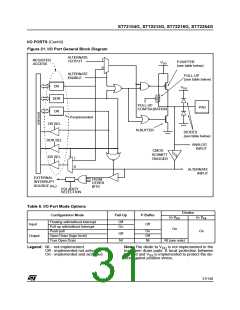
10.3 I/O PORT IMPLEMENTATION
The hardware implementation on each I/O port de-
pends on the settings in the DDR and OR registers
and specific feature of the I/O port such as ADC In-
put or true open drain.
True Open Drain Interrupt Ports
PA6, PA4 (without pull-up)
MODE
DDR
OR
Switching these I/O ports from one state to anoth-
er should be done in a sequence that prevents un-
wanted side effects. Recommended safe transi-
tions are illustrated in Figure 22 Other transitions
are potentially risky and should be avoided, since
they are likely to present unwanted side-effects
such as spurious interrupt generation.
floating input
0
0
1
0
1
X
floating interrupt input
open drain (high sink ports)
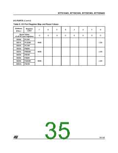
Table 8. Port Configuration
Input (DDR = 0)
Output (DDR = 1)
Port
Pin name
OR = 0
OR = 1
OR = 0
OR = 1
High-Sink
PA7
floating
floating
floating
floating
floating
floating
floating
pull-up interrupt
floating interrupt
pull-up interrupt
floating interrupt
pull-up interrupt
pull-up interrupt
pull-up interrupt
open drain
push-pull
PA6
true open-drain
Port A
PA5
open drain
push-pull
Yes
PA4
true open-drain
PA3:0
PB7:0
PC7:0
open drain
open drain
open drain
push-pull
push-pull
push-pull
Port B
Port C
No
33/140

 ETC [ ETC ]