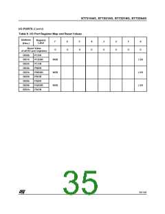
ST72104G, ST72215G, ST72216G, ST72254G
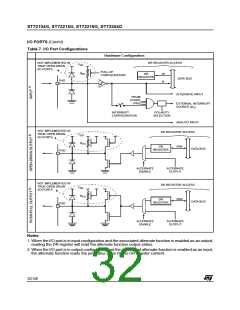
I/O PORTS (Cont’d)
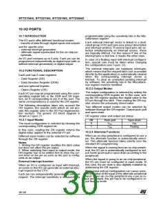
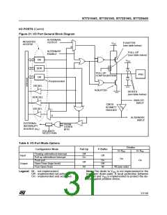
Figure 21. I/O Port General Block Diagram
ALTERNATE
OUTPUT
1
0
REGISTER
ACCESS
P-BUFFER
(see table below)
V
DD
ALTERNATE
ENABLE
PULL-UP
(see table below)
DR
DDR
OR
V
DD
PULL-UP
CONFIGURATION
PAD
If implemented
OR SEL
DDR SEL
DR SEL
N-BUFFER
DIODES
(see table below)
ANALOG
INPUT
CMOS
SCHMITT
TRIGGER
1
0
ALTERNATE
INPUT
EXTERNAL
INTERRUPT
SOURCE (ei )
FROM
OTHER
BITS
x
POLARITY
SELECTION
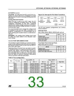
Table 6. I/O Port Mode Options
Configuration Mode
Diodes
Pull-Up
P-Buffer
to V
to V
SS
DD
Floating with/without Interrupt
Pull-up with/without Interrupt
Push-pull
Off
On
Input
Off
On
On
Off
On
Off
NI
Output
Open Drain (logic level)
True Open Drain
NI
NI (see note)
Legend: NI - not implemented
Off - implemented not activated
On - implemented and activated
Note: The diode to V
is not implemented in the
DD
true open drain pads. A local protection between
the pad and V is implemented to protect the de-
SS
vice against positive stress.
31/140

 ETC [ ETC ]