ST6200C/ST6201C/ST6203C
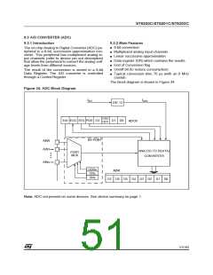
A/D CONVERTER (Cont’d)
9.3.3 Functional description
9.3.3.4 Software procedure
9.3.3.1 Analog Power Supply
Refer to the Control register (ADCR) and Data reg-
ister (ADR) in Section 9.3.7 for the bit definitions.
The high and low level reference voltage pins are
internally connected to the V and V pins.
Analog input configuration
DD
SS
Conversion accuracy may therefore be impacted
by voltage drops and noise in the event of heavily
loaded or badly decoupled power supply lines.
The analog input must be configured through the
Port Control registers (DDRx, ORx and DRx). Re-
fer to the I/O port chapter.
9.3.3.2 Digital A/D Conversion Result
ADC configuration
The conversion is monotonic, meaning that the re-
sult never decreases if the analog input does not
and never increases if the analog input does not.
In the ADCR register:
– Reset the PDS bit to power on the ADC. This bit
must be set at least one instruction before the
beginning of the conversion to allow stabilisation
of the A/D converter.
If the input voltage (V ) is greater than or equal
AIN
to V
(high-level voltage reference) then the
DDA
conversion result in the DR register is FFh (full
scale) without overflow indication.
– Set the EAI bit to enable the ADC interrupt if
needed.
If input voltage (V ) is lower than or equal to
AIN
ADC conversion
V
(low-level voltage reference) then the con-
SSA
In the ADCR register:
version result in the DR register is 00h.
– Set the STA bit to start a conversion. This auto-
matically clears (resets to “0”) the End Of Con-
version Bit (EOC).
The A/D converter is linear and the digital result of
the conversion is stored in the ADR register. The
accuracy of the conversion is described in the par-
ametric section.
When a conversion is complete
R
is the maximum recommended impedance
– The EOC bit is set by hardware to flag that con-
version is complete and that the data in the ADC
data conversion register is valid.
AIN
for an analog input signal. If the impedance is too
high, this will result in a loss of accuracy due to
leakage and sampling not being completed in the
allocated time. Refer to the electrical characteris-
tics chapter for more details.
– An interrupt is generated if the EAI bit was set
Setting the STA bit will start a new count and will
clear the EOC bit (thus clearing the interrupt con-
dition)
With an oscillator clock frequency less than
1.2MHz, conversion accuracy is decreased.
Note:
9.3.3.3 Analog input selection
Setting the STA bit must be done by a different in-
struction from the instruction that powers-on the
ADC (setting the PDS bit) in order to make sure
the voltage to be converted is present on the pin.
Selection of the input pin is done by configuring
the related I/O line as an analog input via the Data
Direction, Option and Data registers (refer to I/O
ports description for additional information).
Each conversion has to be separately initiated by
writing to the STA bit.
Warning: Only one I/O line must be configured as
an analog input at any time. The user must avoid
any situation in which more than one I/O pin is se-
lected as an analog input simultaneously, because
they will be shorted internally.
The STA bit is continuously scanned so that, if the
user sets it to “1” while a previous conversion is in
progress, a new conversion is started before com-
pleting the previous one. The start bit (STA) is a
write only bit, any attempt to read it will show a log-
ical “0”.
52/104
1

 ETC [ ETC ]