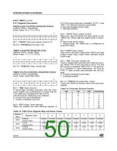
ST6200C/ST6201C/ST6203C
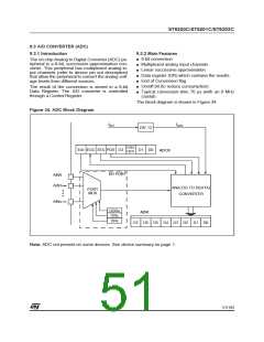
A/D CONVERTER (Cont’d)
9.3.4 Recommendations
bances and power supply variations due to output
switching. Nevertheless, the WAIT instruction
should be executed as soon as possible after the
beginning of the conversion, because execution of
the WAIT instruction may cause a small variation
The following six notes provide additional informa-
tion on using the A/D converter.
1.The A/D converter does not feature a sample
and hold circuit. The analog voltage to be meas-
ured should therefore be stable during the entire
conversion cycle. Voltage variation should not ex-
ceed ±1/2 LSB for optimum conversion accuracy.
A low pass filter may be used at the analog input
pins to reduce input voltage variation during con-
version.
of the V voltage. The negative effect of this var-
DD
iation is minimized at the beginning of the conver-
sion when the converter is less sensitive, rather
than at the end of conversion, when the least sig-
nificant bits are determined.
The best configuration, from an accuracy stand-
point, is WAIT mode with the Timer stopped. In
this case only the ADC peripheral and the oscilla-
tor are then still working. The MCU must be woken
up from WAIT mode by the ADC interrupt at the
end of the conversion. The microcontroller can
also be woken up by the Timer interrupt, but this
means the Timer must be running and the result-
ing noise could affect conversion accuracy.
2. When selected as an analog channel, the input
pin is internally connected to a capacitor C of
ad
typically 9pF. For maximum accuracy, this capaci-
tor must be fully charged at the beginning of con-
version. In the worst case, conversion starts one
instruction (6.5 µs) after the channel has been se-
lected. The impedance of the analog voltage
source (ASI) in worst case conditions, is calculat-
ed using the following formula:
Caution: When an I/O pin is used as an analog in-
put, A/D conversion accuracy will be impaired if
6.5µs = 9 x C x ASI
ad
(capacitor charged to over 99.9%), i.e. 30 kΩ in-
negative current injections (V < V ) occur from
INJ
SS
cluding a 50% guardband.
adjacent I/O pins with analog input capability. Re-
fer to Figure 35. To avoid this:
The ASI can be higher if C has been charged for
ad
a longer period by adding instructions before the
start of conversion (adding more than 26 CPU cy-
cles is pointless).
– Use another I/O port located further away from
the analog pin, preferably not multiplexed on the
A/D converter
3. Since the ADC is on the same chip as the micro-
processor, the user should not switch heavily load-
ed output signals during conversion, if high preci-
sion is required. Such switching will affect the sup-
ply voltages used as analog references.
– Increase the input resistance R
current injections)and reduce R
conversion accuracy).
(to reduce the
IN J
(to preserve
ADC
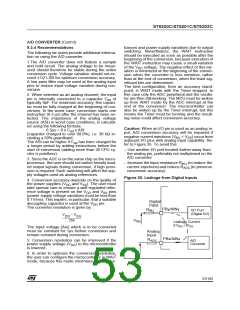
Figure 35. Leakage from Digital Inputs
4. Conversion accuracy depends on the quality of
the power supplies (V and V ). The user must
DD
SS
take special care to ensure a well regulated refer-
ence voltage is present on the V and V pins
DD
SS
(power supply voltage variations must be less than
0.1V/ms). This implies, in particular, that a suitable
Digital
Input
decoupling capacitor is used at the V pin.
DD
The converter resolution is given by:
PBy/AINy
R
I/O Port
INJ
(Digital I/O)
V
– V
DD
SS
-------------------------------
256
V
INJ
Leakage Current
if V < V
INJ
SS
The Input voltage (Ain) which is to be converted
must be constant for 1µs before conversion and
remain constant during conversion.
Analog
Input
PBx/AINx
R
5. Conversion resolution can be improved if the
power supply voltage (V ) to the microcontroller
ADC
A/D
Converter
DD
is lowered.
V
AIN
6. In order to optimize the conversion resolution,
the user can configure the microcontroller in WAIT
mode, because this mode minimises noise distur-
53/104
1

 ETC [ ETC ]