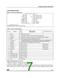
ST6200C/ST6201C/ST6203C
MEMORY MAP (Cont’d)
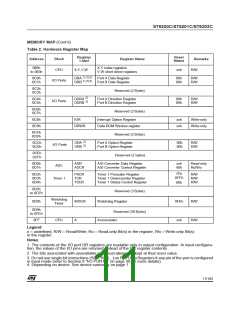
Table 2. Hardware Register Map
Register
Reset
Address
Block
Register Name
X,Y index registers
Remarks
Status
Label
080h
to 083h
CPU
X,Y,V,W
xxh
R/W
V,W short direct registers
1) 2) 3)
0C0h
0C1h
DRA
DRB
Port A Data Register
Port B Data Register
00h
00h
R/W
R/W
I/O Ports
1) 2) 3)
0C2h
0C3h
Reserved (2 Bytes)
2)
0C4h
0C5h
DDRA
DDRB
Port A Direction Register
Port B Direction Register
00h
00h
R/W
R/W
I/O Ports
2)
0C6h
0C7h
Reserved (2 Bytes)
0C8h
0C9h
IOR
Interrupt Option Register
xxh
xxh
Write-only
Write-only
DRWR
Data ROM Window register
0CAh
0CBh
Reserved (2 Bytes)
2)
2)
0CCh
0CDh
ORA
ORB
Port A Option Register
Port B Option Register
00h
00h
R/W
R/W
I/O Ports
0CEh
0CFh
Reserved (2 bytes)
0D0h
0D1h
ADR
ADCR
A/D Converter Data Register
A/D Converter Control Register
xxh
40h
Read-only
Ro/Wo
ADC
7Fh
0FFh
0D2h
0D3h
0D4h
PSCR
TCR
TSCR
Timer 1 Prescaler Register
Timer 1 Downcounter Register
Timer 1 Status Control Register
R/W
R/W
R/W
Timer 1
00h
0FEh
xxh
0D5h
to 0D7h
Reserved (3 Bytes)
Watchdog Register
Watchdog
Timer
0D8h
WDGR
R/W
R/W
0D9h
to 0FEh
Reserved (38 Bytes)
Accumulator
0FF
CPU
A
Legend:
x = undefined, R/W = Read/Write, Ro = Read-only Bit(s) in the register, Wo = Write-only Bit(s)
in the register.
Notes:
1. The contents of the I/O port DR registers are readable only in output configuration. In input configura-
tion, the values of the I/O pins are returned instead of the DR register contents.
2. The bits associated with unavailable pins must always be kept at their reset value.
3. Do not use single-bit instructions (SET, RES...) on Port Data Registers if any pin of the port is configured
in input mode (refer to Section 8 ”I/O PORTS” on page 36 for more details).
4. Depending on device. See device summary on page 1.
11/104
1

 ETC [ ETC ]