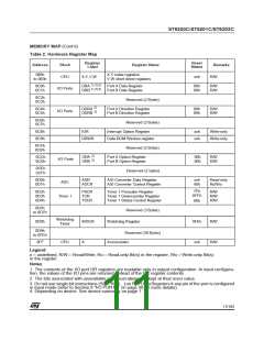
ST6200C/ST6201C/ST6203C
2 PIN DESCRIPTION
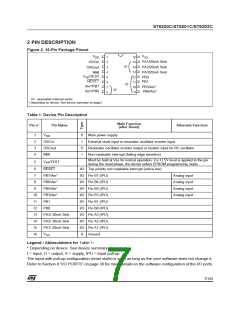
Figure 2. 16-Pin Package Pinout
V
V
SS
1
2
3
4
5
6
7
8
16
15
14
13
12
11
10
9
DD
PA1/20mA Sink
PA2/20mA Sink
OSCin
it1
OSCout
PA3/20mA Sink
NMI
/TEST
V
PB0
PB1
PP
RESET
it2
Ain*/PB7
Ain*/PB6
PB3/Ain*
PB5/Ain*
it2
itX associated interrupt vector
* Depending on device. See device summary on page1.
Table 1. Device Pin Description
Main Function
(after Reset)
Pin n°
Pin Name
Alternate Function
1
2
3
4
V
S
I
Main power supply
External clock input or resonator oscillator inverter input
DD
OSCin
OSCout
NMI
O
I
Resonator oscillator inverter output or resistor input for RC oscillator
Non maskable interrupt (falling edge sensitive)
Must be held at Vss for normal operation, if a 12.5V level is applied to the pin
during the reset phase, the device enters EPROM programming mode.
5
V
/TEST
PP
6
RESET
I/O Top priority non maskable interrupt (active low)
I/O Pin B7 (IPU)
7
PB7/Ain*
Analog input
Analog input
Analog input
Analog input
8
PB6/Ain*
I/O Pin B6 (IPU)
9
PB5/Ain*
I/O Pin B5 (IPU)
10
11
12
13
14
15
16
PB3/Ain*
I/O Pin B3 (IPU)
PB1
I/O Pin B1 (IPU)
PB0
I/O Pin B0 (IPU)
PA3/ 20mA Sink
PA2/ 20mA Sink
PA1/ 20mA Sink
I/O Pin A3 (IPU)
I/O Pin A2 (IPU)
I/O Pin A1 (IPU)
V
S
Ground
SS
Legend / Abbreviations for Table 1:
* Depending on device. See device summary on page 1.
I = input, O = output, S = supply, IPU = input pull-up
The input with pull-up configuration (reset state) is valid as long as the user software does not change it.
Refer to Section 8 ”I/O PORTS” on page 36 for more details on the software configuration of the I/O ports.
7/104

 ETC [ ETC ]