ST6200C/ST6201C/ST6203C
MEMORY MAP (Cont’d)
3.1.6.2 Data ROM Window memory addressing
tion is automatically handled by the ST6 develop-
ment tools.
In cases where some data (look-up tables for ex-
ample) are stored in program memory, reading
these data requires the use of the Data ROM win-
dow mechanism. To do this:
Please refer to the user manual of the correspod-
ing tool.
3.1.6.3 Recommendations
1. The DRWR register has to be loaded with the
64-byte block number where the data are located
(in program memory). This number also gives the
start address of the block.
Care is required when handling the DRWR regis-
ter as it is write only. For this reason, the DRWR
contents should not be changed while executing
an interrupt service routine, as the service routine
cannot save and then restore the register’s previ-
ous contents. If it is impossible to avoid writing to
the DRWR during the interrupt service routine, an
image of the register must be saved in a RAM lo-
cation, and each time the program writes to the
DRWR, it must also write to the image register.
The image register must be written first so that, if
an interrupt occurs between the two instructions,
the DRWR is not affected.
2. Then, the offset address of the byte in the Data
ROM Window (corresponding to the offset in the
64-byte block in program memory) has to be load-
ed in a register (A, X,...).
When the above two steps are completed, the
data can be read.
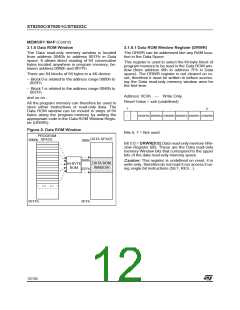
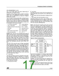
To understand how to determine the DRWR and
the content of the register, please refer to the ex-
ample shown in Figure 6. In any case the calcula-
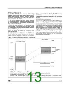
Figure 6. Data ROM Window Memory Addressing
DATA SPACE
000h
PROGRAM SPACE
0000h
040h
OFFSET
21h
DATA
061h
07Fh
0400h
64 bytes
OFFSET
0421h
DATA
DRWR
0FFh
10h
07FFh
DATA address in Program memory : 421h
DRWR content : 421h / 3Fh (64) = 10H data is located in 64-bytes window number 10h
64-byte window start address : 10h x 3Fh = 400h
Register (A, X,...)content : Offset = (421h - 400h) + 40h ( Data ROM Window start address in data space) = 61h
13/104
1

 ETC [ ETC ]