RDA Microelectronics, Inc.
RDA5807SP FM Tuner V1.0
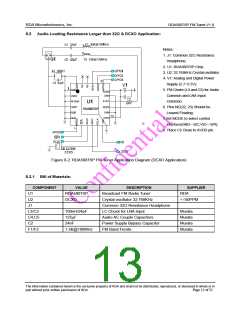
7
Pins Description
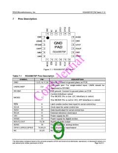
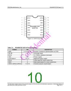
Figure 7-1. RDA5807SP Top View
Table 7-1
RDA5807SP Pins Description
SYMBOL
PIN
DESCRIPTION
GND
1,5,6,14,17,24 Ground. Connect to ground plane on PCB
LNA input port. For single-ended input, LNAN should be
LNAN,LNAP
RFGND
2,4
3
connected to RFGND
LNA ground. Connect to ground plane on PCB
Control Interface select
The MODE Pin is low ,I2C Interface is select.
MODE
7
The MODE Pin is set to VIO, SPI Interface is select.
SEN
8
9
Latch enable (active low) input for serial control bus
Clock input for serial control bus
Data input/output for serial control bus
External reference clock input
Power supply for I/O
SCLK
SDIO
10
RCLK
11
VIO
12
DVDD
13
Power supply for digital section
Right/Left audio output
ROUT,LOUT
15,16
18
AVDD
Power supply for analog section
General purpose input/output
No Connect
GPIO1,GPIO2,GPIO3
NC
19,20,21
22,23
The information contained herein is the exclusive property of RDA and shall not be distributed, reproduced, or disclosed in whole or in
part without prior written permission of RDA.
Page 8 of 21

 ETC [ ETC ]