RDA Microelectronics, Inc.
RDA5807SP FM Tuner V1.0
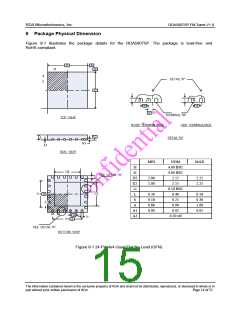
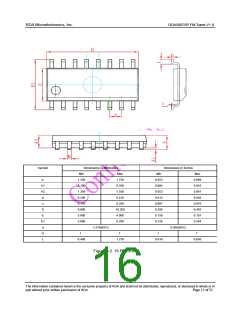
8
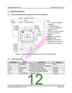
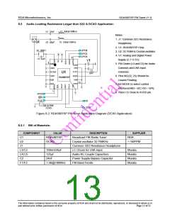
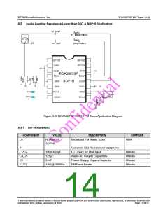
Application Diagram
8.1 Audio Loading Resistance Larger than 32Ω & TCXO Application:
Notes:
1. J1: Common 32Ω Resistance
Headphone;
2. U1: RDA5807SP Chip;
3. V1: Analog and Digital Power
Supply (2.7~5.5V);
4. FM Choke (L3 and C3) for Audio
Common and LNA Input
Common;
5. Pins NC(22, 23), Should be
Leaved Floating;
6.Set MODE to select control
interface(GND—I2C,VIO—SPI);
6. Place C6 Close to AVDD pin.
Figure 8-1. RDA5807SP FM Tuner Application Diagram (TCXO Application)
8.1.1 Bill of Materials:
COMPONENT
U1
VALUE
DESCRIPTION
Broadcast FM Radio Tuner
Common 32Ω Resistance Headphone
LC Chock for LNA Input
SUPPLIER
RDA
RDA5807SP
J1
L3/C3
C4,C5
C6
100nH/24pF
125µF
Murata
Murata
Murata
Murata
Audio AC Couple Capacitors
Power Supply Bypass Capacitor
FM Band Ferrite
24nF
F1/F2
1.5K@100MHz
The information contained herein is the exclusive property of RDA and shall not be distributed, reproduced, or disclosed in whole or in
part without prior written permission of RDA.
Page 11 of 21

 ETC [ ETC ]