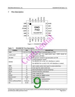
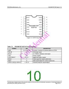
RDA Microelectronics, Inc.
RDA5807SP FM Tuner V1.0
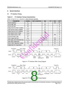
6
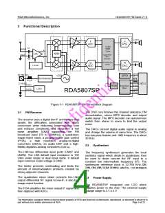
Serial Interface
6.1
I2C Interface Timing
Table 6-1
I2C Interface Timing Characteristics
(VDD = 2.7 to 5.5 V, TA = -25 to 85 °C, unless otherwise specified)
PARAMETER
SCLK Frequency
SYMBOL
fscl
TEST CONDITION
MIN
TYP
MAX
UNIT
KHz
ms
0
-
-
-
-
-
-
-
-
-
-
-
-
-
400
SCLK High Time
0.6
-
thigh
SCLK Low Time
1.3
-
-
tlow
ms
Setup Time for START Condition
Hold Time for START Condition
Setup Time for STOP Condition
SDIO Input to SCLK↑ Setup
SDIO Input to SCLK↓ Hold
STOP to START Time
0.6
tsu:sta
thd:sta
tsu:sto
tsu:dat
thd:dat
tbuf
ms
0.6
-
ms
0.6
-
ms
100
-
ns
0
900
-
ns
1.3
ms
SDIO Output Fall Time
20+0.1Cb
250
300
50
50
5
ns
tf:out
SDIO Input, SCLK Rise/Fall Time
Input Spike Suppression
SCLK, SDIO Capacitive Loading
Digital Input Pin Capacitance
20+0.1Cb
ns
tr:in / tf:in
tsp
-
-
ns
pF
pF
Cb
Figure 6-1. I2C Interface Write Timing Diagram
Figure 6-2. I2C Interface Read Timing Diagram
The information contained herein is the exclusive property of RDA and shall not be distributed, reproduced, or disclosed in whole or in
part without prior written permission of RDA.
Page 7 of 21

 ETC [ ETC ]