RDA Microelectronics, Inc.
3.4 RESET and Control Interface select
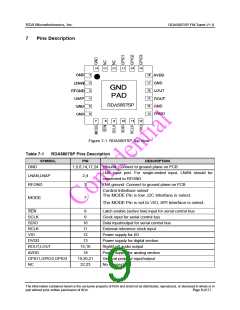
RDA5807SP FM Tuner V1.0
after command byte from MCU, RDA5807SP
sends out the first register high byte, then the first
register low byte, then the second register high
byte, till receives NACK from MCU. MCU gives out
ACK for data bytes besides last data byte. MCU
gives out NACK for last data byte, and then
RDA5807SP will return the bus to MCU, and MCU
will give out STOP condition.
The RDA5807SP is RESET itself When VIO is
Power up. And also support soft reset. The control
interface is select by MODE Pin. The MODE Pin
is low ,I2C Interface is select. The MODE Pin is
set to VIO, SPI Interface is select.
The RDA5807SP could enter into a power-down
mode to reduce power consumption.
The RDA5807SP supported two type I2C
In power-down mode, analog and digital circuitry
are both disabled, while maintaining register
interface:RDA5807SP Mode and TEA5767 Mode.
The different register defined in different interface
configuration and keeping control interface active.
Mode.
Details refer to RDA5807SP Programming Guide.
Details refer to RDA5807SP Programming Guide.
3.5
Control Interface
3.6
GPIO Outputs
The RDA5807SP supports I2C control interface.
User could program the chip through the bus.
The RDA5807SP has three GPIOs and only used
in RDA5807SP Mode. The function of GPIOs
could programmed with bits GPIO1[1:0],
GPIO2[1:0], GPIO3[1:0] and I2SEN.
The I2C interface is compliant to I2C Bus
Specification 2.1. It includes two pins: SCLK and
SDIO. An I2C interface transfer begins with
START condition, a command byte and data bytes,
each byte has a followed ACK (or NACK) bit, and
ends with STOP condition. The command byte
includes a 7-bit chip address and an R/W bit. The
ACK (or NACK) is always sent out by receiver.
When in write transfer, data bytes is written out
from MCU, and when in read transfer, data bytes
is read out from RDA5807SP. There is no visible
register address in I2C interface transfers.
If I2SEN is set to low, GPIO pins could be
programmed to output low or high or high-Z, or be
programmed to output interrupt and stereo
indicator with bits GPIO1[1:0], GPIO2[1:0],
GPIO3[1:0]. GPIO2 could be programmed to
output a low interrupt (interrupt will be generated
only with interrupt enable bit STCIEN is set to high)
when seek/tune process completes. GPIO3 could
be programmed to output stereo indicator bit ST.
Constant low, high or high-Z functionality is
available regardless of the state of VA and VD
supplies or the ENABLE bit.
RDA5807SP always gives out ACK after every
byte, and MCU gives out STOP condition when
register programming is finished. For read transfer,
SCK
LEFT CHANNEL
RIGHT CHANNEL
WS
1 SCK
1 SCK
MSB
LSB
MSB
LSB
SD
Figure 3-2. I2S Digital Audio Format
The information contained herein is the exclusive property of RDA and shall not be distributed, reproduced, or disclosed in whole or in
part without prior written permission of RDA.
Page 4 of 21

 ETC [ ETC ]