®
PMD-100
PMD-100 Process Decoder
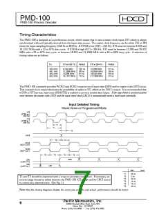
Data Input
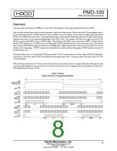
The input data word format is MSB first, 16 to 24-bit left justified or 16 bit right justified (selected by JUST).
Left and right channel data words are input alternately, with the left channel first. Refer to the Input Timing diagram below.
Each serial input data bit is shifted into the serial to parallel conversion register on the rising or falling edge (selected by
BCPL) of the BCKI bit clock input. The parallel data output is alternatively latched into the left and right channel input
registers respectively on the rising and falling edges of the LRCI clock. The number of BCKI active edges must be 16, 18,
20, 24, or more while LRCI is low or LRCI is high. The polarity of the LRCI clock is selected by LRPL. In Stand-Alone
Mode, LRPL default is low. If LRPL is low, the rising edge of LRCI indicates the start of the data input cycle. Left channel
data is input while LRCI is high and latched on the falling edge. Right channel data is then input while LRCI is low, and
latched on the rising edge. If LRPL is high, the clock polarity is reversed and the falling edge of LRCI indicates the start of
the data input cycle.
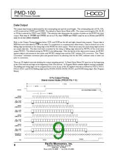
The group (data input-to-output) delay is 83 input samples. This is measured from the active edge of LRCI preceding the
input data, to the active edge of LRCI preceding the same phase output data. The group delay is the same with 2 Fs, 4 Fs
or 8 Fs operation.
When the input data format is I2S, the word clock is received one bit clock too early. A simple method for delaying the word
clock for proper timing is to use a logic device to delay the word clock until it is triggered by the rising edge of the bit clock.
(See Application Notes pg.s 16-20).
Input Timing
Stand-Alone or Programmed Mode
RIGHT
RIGHT
Pacific Microsonics, Inc.
7
32990 Alvarado Niles Road, Suite 910
Union City, CA 94587
Phone (510) 475-8000
Fax (510) 475-8005

 ETC [ ETC ]