AD7804/AD7805/AD7808/AD7809
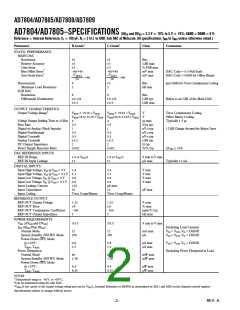
AD7808/AD7809–SPECIFICATIONS (AV and DV
DD = 3.3 V ؎ 10% to 5 V ؎ 10%; AGND = DGND = 0 V;
Reference = Internal Reference; CL = 100 pF; RL = 2 k⍀ to GND. Sub DAC at Midscale. All specifications TMIN to TMAX unless otherwise noted.)
DD
Parameter
B Grade1
Units
Comments
STATIC PERFORMANCE
MAIN DAC
Resolution
10
±4
±3
±60
±35
9
Bits
Relative Accuracy
Gain Error
LSB max
% FSR max
mV max
mV max
Bits
Bias Offset Error2
Zero-Scale Error
Monotonicity
DAC Code = 0.5 Full Scale
DAC Code = 000H for Offset Binary
and 200H for Twos Complement
Coding
Minimum Load Resistance
SUB DAC
2
kΩ min
Resolution
8
Bits
Differential Nonlinearity
±0.125
±0.5
LSB typ
LSB max
Refers to an LSB of the Main DAC
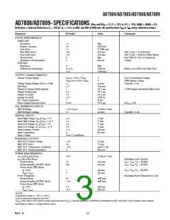
OUTPUT CHARACTERISTICS
Output Voltage Range3
V
BIAS ± 15/16 × VBIAS
V
V
Twos Complement Coding
Offset Binary Coding
Typically 1.5 µs
VBIAS/16 to 31/16 × VBIAS
4
Voltage Output Settling Time to 10 Bits
Slew Rate
Digital-to-Analog Glitch Impulse
Digital Feedthrough
Digital Crosstalk
Analog Crosstalk
µs max
V/µs typ
nV-s typ
nV-s typ
nV-s typ
LSB typ
Ω typ
2.5
1
0.5
0.5
±0.2
2
1 LSB Change Around the Major Carry
DC Output Impedance
Power Supply Rejection Ratio
0.002
%/% typ
∆VDD ± 10%
DAC REFERENCE INPUTS
REF IN Range
1.0 to VDD/2
V min to V max
REF IN Input Leakage
±1
µA max
Typically ±1 nA
DIGITAL INPUTS
Input High Voltage, VIH @ VDD = 5 V
Input High Voltage, VIH @ VDD = 3.3 V
Input Low Voltage, VIL @ VDD = 5 V
Input Low Voltage, VIL @ VDD = 3.3 V
Input Leakage Current
2.4
2.1
0.8
0.6
±10
8
V min
V min
V max
V max
µA max
pF max
Input Capacitance
Input Coding
Twos Comp/Binary
REFERENCE OUTPUT
REF OUT Output Voltage
REF OUT Error
1.23
±8
V nom
% max
REF OUT Temperature Coefficient
REF OUT Output Impedance
–100
5
ppm/°C typ
kΩ nom
POWER REQUIREMENTS
VDD (AVDD and DVDD
)
3/5.5
V min to V max
IDD (AIDD Plus DIDD
Normal Mode
System Standby (SSTBY) Mode
Power-Down (PD) Mode
@ +25°C
)
Excluding Load Currents
VIH = VDD, VIL = DGND
VIH = VDD, VIL = DGND
18
250
mA max
µA max
1
3
µA max
µA max
VIH = VDD, VIL = DGND
TMIN–TMAX
Power Dissipation
Normal Mode
System Standby (SSTBY) Mode
Power-Down (PD) Mode
@ +25°C
Excluding Power Dissipated in Load
99
1.38
mW max
mW max
5.5
16.5
µW max
µW max
TMIN–TMAX
NOTES
1Temperature range is –40°C to +85°C.
2Can be minimized using the Sub DAC.
3VBIAS is the center of the output voltage swing and can be VDD/2, Internal Reference or REFIN as determined by MX1 and MX0 in the channel control register.
Specifications subject to change without notice.
–3–
REV. A

 ETC [ ETC ]