7
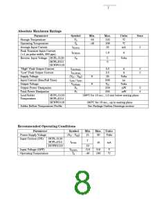
Absolute Maximum Ratings
Parameter
Storage Temperature
Operating Temperature
Average Input Current
Symbol
TS
TA
IF(AVG)
Min.
-55
-40
Max.
125
100
25
Units
°C
°C
Note
mA
1
Peak Transient Input Current
(<1 µs pulse width, 300 pps)
Reverse Input Voltage HCPL-3120
IF(TRAN)
VR
1.0
A
5
3
Volts
HCPL-J312
HCNW3120
“High” Peak Output Current
“Low” Peak Output Current
Supply Voltage
Input Current (Rise/Fall Time)
Output Voltage
IOH(PEAK)
IOL(PEAK)
(VCC - VEE)
tr(IN) / tf(IN)
VO(PEAK)
PO
2.5
2.5
35
500
VCC
250
295
A
A
Volts
ns
Volts
mW
mW
2
2
0
0
Output Power Dissipation
Total Power Dissipation
3
4
PT
Lead Solder
Temperature
HCPL-3120
HCPL-J312
260°C for 10 sec., 1.6 mm below seating plane
HCNW3120
260°C for 10 sec., up to seating plane
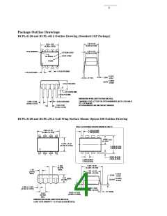
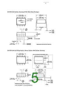
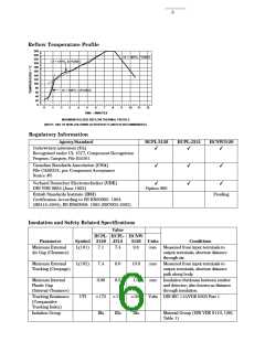
Solder Reflow Temperature Profile
See Package Outline Drawings section
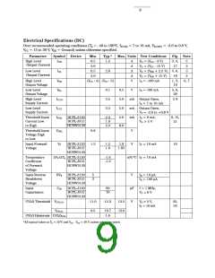
Recommended Operating Conditions
Parameter
Power Supply Voltage
Input Current (ON)
Symbol
(VCC - VEE)
Min.
15
Max. Units
30
Volts
HCPL-3120
HCPL-J312
7
IF(ON)
16
mA
HCNW3120
10
-3.0
-40
Input Voltage (OFF)
VF(OFF)
TA
0.8
V
Operating Temperature
100
°C

 ETC [ ETC ]