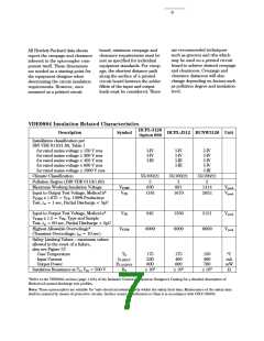
6
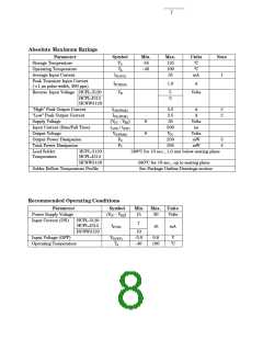
are recommended techniques
such as grooves and ribs which
may be used on a printed circuit
board to achieve desired creepage
and clearances. Creepage and
clearance distances will also
change depending on factors such
as pollution degree and insulation
level.
board, minimum creepage and
clearance requirements must be
met as specified for individual
equipment standards. For creep-
age, the shortest distance path
along the surface of a printed
circuit board between the solder
fillets of the input and output
leads must be considered. There
All Hewlett-Packard data sheets
report the creepage and clearance
inherent to the optocoupler com-
ponent itself. These dimensions
are needed as a starting point for
the equipment designer when
determining the circuit insulation
requirements. However, once
mounted on a printed circuit
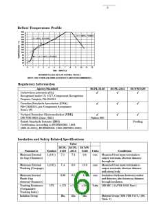
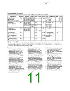
VDE0884 Insulation Related Characteristics
HCPL-3120
Option 060
Description
Symbol
HCPL-J312 HCNW3120 Unit
Installation classification per
DIN VDE 0110/1.89, Table 1
for rated mains voltage ≤ 150 V rms
for rated mains voltage ≤ 300 V rms
for rated mains voltage ≤ 450 V rms
for rated mains voltage ≤ 600 V rms
for rated mains voltage ≤ 1000 V rms
Climatic Classification
Pollution Degree (DIN VDE 0110/1.89)
Maximum Working Insulation Voltage
Input to Output Test Voltage, Method b*
VIORM x 1.875 = VPR, 100% Production
Test, tm = 1 sec, Partial Discharge < 5pC
I-IV
I-IV
I-III
I-IV
I-IV
I-III
I-III
I-IV
I-IV
I-IV
I-IV
I-III
55/100/21
2
55/100/21
2
55/100/21
2
VIORM
VPR
630
1181
891
1670
1414
2652
Vpeak
Vpeak
Input to Output Test Voltage, Method a*
VIORM x 1.5 = VPR, Type and Sample
Test, tm = 60 sec, Partial Discharge < 5pC
Highest Allowable Overvoltage*
(Transient Overvoltage, tini = 10 sec)
Safety Limiting Values – maximum values
allowed in the event of a failure,
also see Figure 37.
VPR
945
1336
6000
2121
8000
Vpeak
VIOTM
6000
Vpeak
Case Temperature
Input Current
Output Power
TS
IS INPUT
PS OUTPUT
RS
175
230
600
≥ 109
175
400
600
≥ 109
150
400
700
≥ 109
°C
mA
mW
Ω
Insulation Resistance at TS, VIO = 500 V
*Refer to the VDE0884 section (page 1-6/8) of the Isolation Control Component Designer's Catalog for a detailed description of
Method a/b partial discharge test profiles.
Note: These optocouplers are suitable for “safe electrical isolation” only within the safety limit data. Maintenance of the safety data
shall be ensured by means of protective circuits. Surface mount classification is Class A in accordance with CECC 00802.

 ETC [ ETC ]