10
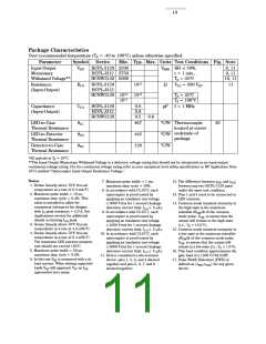
Package Characteristics
Over recommended temperature (TA = -40 to 100°C) unless otherwise specified.
Parameter
Symbol
Device
Min. Typ. Max. Units Test Conditions Fig. Note
Input-Output
Momentary
Withstand Voltage**
Resistance
V
HCPL-3120 2500
HCPL-J312 3750
HCNW3120 5000
VRMS RH < 50%,
t = 1 min.,
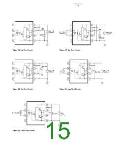
8, 11
9, 11
10, 11
ISO
TA = 25°C
RI-O
HCPL-3120
HCPL-J312
1012
Ω
VI-O = 500 VDC
11
(Input-Output)
HCNW3120 1012 1013
1011
TA = 25°C
TA = 100°C
Capacitance
(Input-Output)
CI-O
HCPL-3120
HCPL-J312
HCNW3120
0.6
0.8
0.5
pF
f = 1 MHz
0.6
LED-to-Case
Thermal Resistance
LED-to-Detector
Thermal Resistance
θLC
θLD
θDC
467
442
126
°C/W Thermocouple
28
located at center
underside of
package
°C/W
°C/W
Detector-to-Case
Thermal Resistance
*All typicals at T = 25°C.
A
**The Input-Output Momentary Withstand Voltage is a dielectric voltage rating that should not be interpreted as an input-output
continuous voltage rating. For the continuous voltage rating refer to your equipment level safety specification or HP Application Note
1074 entitled “Optocoupler Input-Output Endurance Voltage.”
Notes:
7. Maximum pulse width = 1 ms,
maximum duty cycle = 20%.
8. In accordance with UL1577, each
optocoupler is proof tested by
12. The difference between tPHL and tPLH
between any two HCPL-3120 parts
under the same test condition.
13. Pins 1 and 4 need to be connected to
LED common.
14. Common mode transient immunity in
the high state is the maximum
tolerable dVCM/dt of the common
mode pulse, VCM, to assure that the
output will remain in the high state
(i.e., VO > 15.0 V).
15. Common mode transient immunity in
a low state is the maximum tolerable
dVCM/dt of the common mode pulse,
VCM, to assure that the output will
remain in a low state (i.e., VO < 1.0 V).
16. This load condition approximates the
gate load of a 1200 V/75A IGBT.
17. Pulse Width Distortion (PWD) is
defined as |tPHL-tPLH| for any given
device.
1. Derate linearly above 70°C free-air
temperature at a rate of 0.3 mA/°C.
2. Maximum pulse width = 10 µs,
maximum duty cycle = 0.2%. This
value is intended to allow for
component tolerances for designs
with IO peak minimum = 2.0 A. See
Applications section for additional
details on limiting IOH peak.
3. Derate linearly above 70°C free-air
temperature at a rate of 4.8 mW/°C.
4. Derate linearly above 70°C free-air
temperature at a rate of 5.4 mW/°C.
The maximum LED junction tempera-
ture should not exceed 125°C.
5. Maximum pulse width = 50 µs,
maximum duty cycle = 0.5%.
6. In this test VOH is measured with a dc
load current. When driving capacitive
loads VOH will approach VCC as IOH
approaches zero amps.
applying an insulation test voltage
≥ 3000 Vrms for 1 second (leakage
detection current limit, II-O ≤ 5 µA).
9. In accordance with UL1577, each
optocoupler is proof tested by
applying an insulation test voltage
≥ 4500 Vrms for 1 second (leakage
detection current limit, II-O ≤ 5 µA).
10. In accordance with UL1577, each
optocoupler is proof tested by
applying an insulation test voltage
≥ 6000 Vrms for 1 second (leakage
detection current limit, II-O ≤ 5 µA).
11. Device considered a two-terminal
device: pins 1, 2, 3, and 4 shorted
together and pins 5, 6, 7, and 8
shorted together.

 ETC [ ETC ]