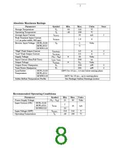
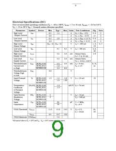
2.0 Amp Output Current IGBT
Gate Drive Optocoupler
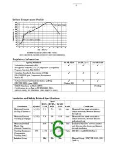
Technical Data
HCPL-3120
HCPL-J312
HCNW3120
Features
• 2.0 A Minimum Peak Output
Current
• 15 kV/µs Minimum Common
Mode Rejection (CMR) at
VCM = 1500 V
• 0.5 V Maximum Low Level
Output Voltage (VOL)
Eliminates Need for Negative
Gate Drive
Applications
• IGBT/MOSFET Gate Drive
• AC/Brushless DC Motor
Drives
• Industrial Inverters
CSA Approval
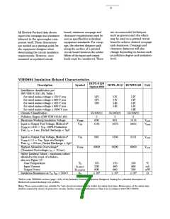
VDE 0884 Approved
VIORM = 630 Vpeak for
HCPL-3120 (Option 060)
VIORM = 891 Vpeak for
HCPL-J312
• Switch Mode Power
Supplies
VIORM = 1414 Vpeak for
HCNW3120
BSI Certified (HCNW3120
only) (Pending)
• ICC = 5 mA Maximum Supply
Current
Functional Diagram
• Under Voltage Lock-Out
Protection (UVLO) with
Hysteresis
• Wide Operating VCC Range:
15 to 30 Volts
• 500 ns Maximum Switching
Speeds
• Industrial Temperature
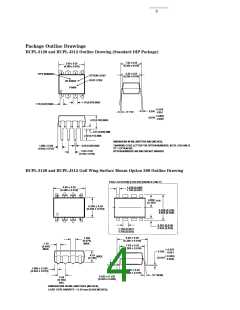
HCPL-3120/J312
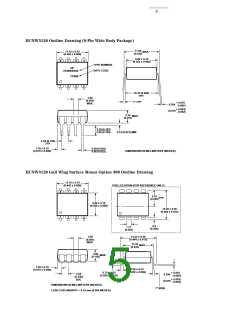
HCNW3120
N/C
ANODE
CATHODE
N/C
1
8
V
V
V
V
N/C
1
8
V
V
CC
CC
O
2
3
4
7
6
5
2
3
4
7
6
5
ANODE
CATHODE
N/C
O
N/C
O
V
EE
EE
SHIELD
SHIELD
Range: -40°C to 100°C
• Safety Approval
UL Recognized
2500 Vrms for 1 min. for
HCPL-3120
3750 Vrms for 1 min. for
HCPL-J312
5000 Vrms for 1 min. for
HCNW3120
TRUTH TABLE
VCC - VEE
VCC - VEE
“POSITIVE GOING” “NEGATIVE GOING”
LED
OFF
ON
(i.e., TURN-ON)
(i.e., TURN-OFF)
VO
LOW
0 - 30 V
0 - 30 V
0 - 11 V
0 - 9.5 V
LOW
ON
11 - 13.5 V
13.5 - 30 V
9.5 - 12 V
12 - 30 V
TRANSITION
HIGH
ON
A 0.1 µF bypass capacitor must be connected between pins 5 and 8.
CAUTION: It is advised that normal static precautions be taken in handling and assembly of this component
to prevent damage and/or degradation which may be induced by ESD.

 ETC [ ETC ]