PIC12F510/16F506
13.4 Timing Parameter Symbology and Load Conditions
The timing parameter symbols have been created following one of the following formats:
1. TppS2ppS
2. TppS
T
F
Frequency
T Time
Lowercase (pp) and their meanings:
pp
2
To
mc
osc
os
MCLR
ck
cy
drt
io
CLKOUT
Cycle Time
Device Reset Timer
I/O port
Oscillator
OSC1
t0
T0CKI
wdt
Watchdog Timer
Uppercase letters and their meanings:
S
F
H
I
Fall
P
R
V
Z
Period
High
Rise
Invalid (High-impedance)
Low
Valid
L
High-impedance
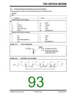
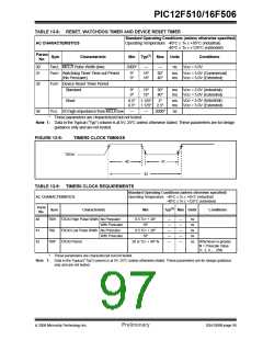
FIGURE 13-5:
LOAD CONDITIONS
Legend:
CL = 50 pF for all pins except OSC2
Pin
Cl
15 pF for OSC2 in XT, HS or LP
modes when external clock
is used to drive OSC1
VSS
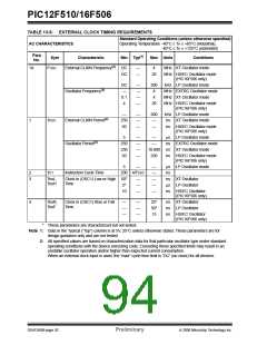
FIGURE 13-6:
EXTERNAL CLOCK TIMING
Q4
Q3
Q4
4
Q1
Q1
Q2
OSC1
1
3
3
4
2
© 2006 Microchip Technology Inc.
Preliminary
DS41268B-page 91

 ETC [ ETC ]