PIC12F510/16F506
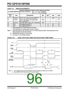
TABLE 13-8: RESET, WATCHDOG TIMER AND DEVICE RESET TIMER
Standard Operating Conditions (unless otherwise specified)
Operating Temperature -40°C ≤ TA ≤ +85°C (industrial)
-40°C ≤ TA ≤ +125°C (extended)
AC CHARACTERISTICS
Param
Sym
No.
Characteristic
Min Typ(1) Max
Units
Conditions
30
31
TMCL MCLR Pulse Width (low)
2000*
—
—
ns
VDD = 5.0V
TWDT Watchdog Timer Time-out Period
(No Prescaler)
9*
9*
18*
18*
30*
40*
ms
ms
VDD = 5.0V (Commercial)
VDD = 5.0V (Extended)
32
34
TDRT Device Reset Timer Period
Standard
9*
9*
18*
18*
30*
40*
ms
ms
VDD = 5.0V (Industrial)
VDD = 5.0V (Extended)
Short
0.5* 1.125*
0.5* 1.125* 2.5*
2*
ms
ms
VDD = 5.0V (Industrial)
VDD = 5.0V (Extended)
TIOZ I/O high-impedance from MCLR low
—
—
2000*
ns
*
These parameters are characterized but not tested.
Note 1: Data in the Typical (“Typ”) column is at 5V, 25°C unless otherwise stated. These parameters are for design
guidance only and are not tested.
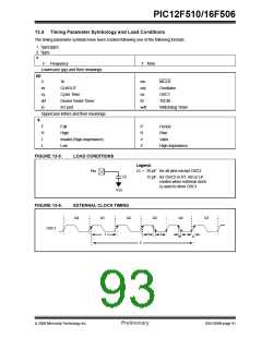
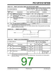
FIGURE 13-9:
TIMER0 CLOCK TIMINGS
T0CKI
40
41
42
TABLE 13-9: TIMER0 CLOCK REQUIREMENTS
Standard Operating Conditions (unless otherwise specified)
Operating Temperature -40°C ≤ TA ≤ +85°C (industrial)
-40°C ≤ TA ≤ +125°C (extended)
AC CHARACTERISTICS
Parm
Sym
No.
(1)
Characteristic
Min
Typ
Max Units
Conditions
40
41
42
Tt0H
Tt0L
Tt0P
T0CKI High Pulse Width No Prescaler
With Prescaler
0.5 TCY + 20*
10*
—
—
—
—
—
—
—
—
—
—
ns
ns
ns
ns
T0CKI Low Pulse Width No Prescaler
With Prescaler
0.5 TCY + 20*
10*
T0CKI Period
20 or TCY + 40* N
ns Whichever is greater.
N = Prescale Value
(1, 2, 4,..., 256)
*
These parameters are characterized but not tested.
Note 1: Data in the Typical (“Typ”) column is at 5V, 25°C unless otherwise stated. These parameters are for design guidance
only and are not tested.
© 2006 Microchip Technology Inc.
Preliminary
DS41268B-page 95

 ETC [ ETC ]