PIC12F510/16F506
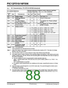
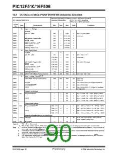
13.3 DC Characteristics: PIC12F510/16F506 (Industrial, Extended)
Standard Operating Conditions (unless otherwise specified)
DC CHARACTERISTICS
Operating Temperature
-40°C ≤ TA ≤ +85°C (industrial)
-40°C ≤ TA ≤ +125°C (extended)
Param
Sym
No.
Characteristic
Min
Typ†
Max
Units
Conditions
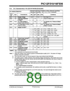
VIL
Input Low Voltage
I/O ports
D030
D030A
D031
D032
D033
D033
D033
with TTL buffer
VSS
VSS
VSS
VSS
VSS
VSS
VSS
—
—
—
—
—
—
—
0.8V
V
V
V
V
V
V
V
For 4.5 ≤ VDD ≤ 5.5V
0.15 VDD
0.15 VDD
0.15 VDD
0.15 VDD
0.3 VDD
0.3 VDD
otherwise
with Schmitt Trigger buffer
MCLR, T0CKI
OSC1 (in EXTRC), EC(1)
OSC1 (in HS)
OSC1 (in XT and LP)
Input High Voltage
I/O ports
VIH
—
—
—
D040
with TTL buffer
2.0
VDD
VDD
V
V
4.5 ≤ VDD ≤ 5.5V
D040A
0.25 VDD
+ 0.8V
0.85 VDD
0.85 VDD
0.85 VDD
0.7 VDD
1.6
Otherwise
D041
D042
D043
D043
D043
D070
with Schmitt Trigger buffer
MCLR, T0CKI
OSC1 (in EXTRC), EC(1)
—
—
VDD
VDD
VDD
VDD
VDD
TBD
V
V
For entire VDD range
—
V
OSC1 (in HS)
—
V
OSC1 (in XT and LP)
—
V
IPUR
IIL
GPIO/PORTB Weak Pull-up Current
Input Leakage Current(2), (3)
GPIO Weak Pull-up Current (GP3)
TBD
250
μA
VDD = 5V, VPIN = VSS
D070
TBD
225
TBD
μA
VDD = 5V
VPIN = 0V
D060
D061A
D063
I/O ports
GP3/RB3/MCLR(4)
—
—
—
—
—
—
±1
±5
±5
μA
μA
μA
Vss ≤ VPIN ≤ VDD, Pin at high-impedance
Vss ≤ VPIN ≤ VDD
OSC1
Vss ≤ VPIN ≤ VDD, XT, HS and LP oscillator
configuration
Output Low Voltage
D080
VOL
I/O ports/CLKOUT
—
—
—
—
—
—
—
—
0.6
0.6
0.6
0.6
V
V
V
V
IOL = 8.5 mA, VDD = 4.5V, –40°C to +85°C
IOL = 7.0 mA, VDD = 4.5V, –40°C to +125°C
IOL = 1.6 mA, VDD = 4.5V, –40°C to +85°C
IOL = 1.2 mA, VDD = 4.5V, –40°C to +125°C
D080A
D083
OSC2
D083A
Output High Voltage
D090
VOH
I/O ports/CLKOUT(3)
VDD – 0.7
VDD – 0.7
VDD – 0.7
VDD – 0.7
—
—
—
—
—
—
—
—
V
V
V
V
IOH = -3.0 mA, VDD = 4.5V, –40°C to +85°C
IOH = -2.5 mA, VDD = 4.5V, –40°C to +125°C
IOH = -1.3 mA, VDD = 4.5V, –40°C to +85°C
IOH = -1.0 mA, VDD = 4.5V, –40°C to +125°C
D090A
D092
OSC2
D092A
Capacitive Loading Specs on Output Pins
COSC2 OSC2 pin
D100
—
—
—
—
15
50
pF
pF
In XT, HS and LP modes when external
clock is used to drive OSC1.
D101
CIO
All I/O pins
Legend:
TBD = To be determined.
†
Data in “Typ” column is at 5V, 25°C unless otherwise stated. These parameters are for design guidance only and are not tested.
Note 1:
In EXTRC oscillator configuration, the OSC1/CLKIN pin is a Schmitt Trigger input. It is not recommended that the PIC12F510/16F506 be
driven with external clock in RC mode.
2:
The leakage current on the MCLR pin is strongly dependent on the applied voltage level. The specified levels represent normal operating
conditions. Higher leakage current may be measured at different input voltages.
Negative current is defined as coming out of the pin.
This specification applies when GP3/MCLR is configured as an input with pull-up disabled. The leakage current of the MCLR circuit is
higher than the standard I/O logic.
3:
4:
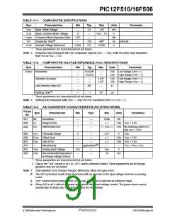
DS41268B-page 88
Preliminary
© 2006 Microchip Technology Inc.

 ETC [ ETC ]