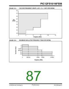
PIC12F510/16F506
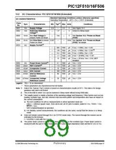
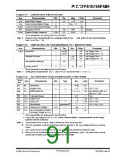
TABLE 13-1: COMPARATOR SPECIFICATIONS
Sym
Characteristics
Input Offset Voltage
Min
Typ
Max
Units
Comments
VOS
VCM
—
0
±3
—
±10
VDD – 1.5
—
mV
V
Input Common Mode Voltage
Common Mode Rejection Ratio
Response Time(1)
CMRR
TRT
+55*
—
—
dB
ns
V
150
0.6
400*
Internal
VIVRF
Internal Voltage Reference
0.550
0.650
*
These parameters are characterized but not tested.
Note 1: Response time measured with one comparator input at (VDD – 1.5)/2, while the other input transitions
from VSS to VDD – 1.5V.
TABLE 13-2: COMPARATOR VOLTAGE REFERENCE (VREF) SPECIFICATIONS
Sym
Characteristics
Min
Typ
Max
Units
Comments
CVRES Resolution
—
—
VDD/24*
VDD/32
—
—
LSb
LSb
Low Range (VRR = 1)
High Range (VRR = 0)
Absolute Accuracy
—
—
—
—
±1/4*
±1/2*
LSb
LSb
Low Range (VRR = 1)
High Range (VRR = 0)
Unit Resistor Value (R)
Settling Time(1)
—
—
2K*
—
Ω
—
—
10*
μs
*
These parameters are characterized but not tested.
Note 1: Settling time measured while VRR = 1and VR<3:0> transitions from 0000to 1111.
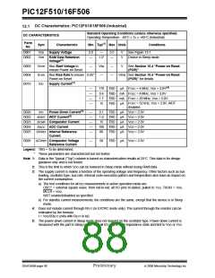
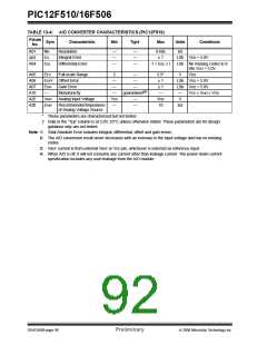
TABLE 13-3: A/D CONVERTER CHARACTERISTICS (PIC12F510/16F506)
Param
Sym
Characteristic
Min
Typ†
Max
Units
Conditions
No.
A01
NR
Resolution
—
—
—
—
—
—
8 bits
± 1
bit
A03
A04
EIL
Integral Error
LSb VDD = 5.0V
EDL
Differential Error
-1 < EDL ≤ 1 LSb No missing codes to 8
bits VDD = 5.0V
A05
A06
A07
A10
A25
A30
EFS
EOFF
EGN
—
Full-scale Range
Offset Error
2
—
—
5.5*
± 1
± 1
—
V
VDD
—
LSb VDD = 5.0V
LSb VDD = 5.0V
Gain Error
—
—
Monotonicity
—
guaranteed(2)
—
V
VSS ≤ VAIN ≤ VDD
VAIN
ZAIN
Analog Input Voltage
VSS
—
—
—
VDD
10
RecommendedImpedance
of Analog Voltage Source
kΩ
*
These parameters are characterized but not tested.
†
Data in the “Typ” column is at 5.0V, 25°C unless otherwise stated. These parameters are for design
guidance only are not tested.
Note 1: Total Absolute Error includes integral, differential, offset and gain errors.
2: The A/D conversion result never decreases with an increase in the input voltage and has no missing
codes.
3: VREF current is from external VREF or VDD pin, whichever is selected as reference input.
4: When A/D is off, it will not consume any current other than leakage current. The power-down current
specification includes any such leakage from the A/D module.
© 2006 Microchip Technology Inc.
Preliminary
DS41268B-page 89

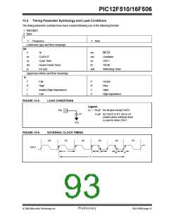
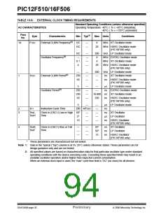
 ETC [ ETC ]