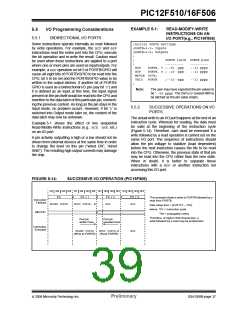
PIC12F510/16F506
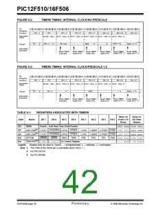
When a prescaler is used, the external clock input is
divided by the asynchronous ripple counter-type
prescaler, so that the prescaler output is symmetrical.
For the external clock to meet the sampling require-
ment, the ripple counter must be taken into account.
Therefore, it is necessary for T0CKI or the comparator
output to have a period of at least 4TOSC (and a small
RC delay of 4Tt0H) divided by the prescaler value. The
only requirement on T0CKI or the comparator output
high and low time is that they do not violate the
minimum pulse width requirement of Tt0H. Refer to
parameters 40, 41 and 42 in the electrical specification
of the desired device.
6.1
Using Timer0 With An External
Clock
When an external clock input is used for Timer0, it must
meet certain requirements. The external clock require-
ment is due to internal phase clock (TOSC) synchroniza-
tion. Also, there is a delay in the actual incrementing of
Timer0 after synchronization.
6.1.1
EXTERNAL CLOCK
SYNCHRONIZATION
When no prescaler is used, the external clock input is
the same as the prescaler output. The synchronization
of an external clock with the internal phase clocks is
accomplished by sampling the prescaler output on the
Q2 and Q4 cycles of the internal phase clocks
(Figure 6-4). Therefore, it is necessary for T0CKI or the
comparator output to be high for at least 2TOSC (and a
small RC delay of 2Tt0H) and low for at least 2TOSC
(and a small RC delay of 2Tt0H). Refer to the electrical
specification of the desired device.
6.1.2
TIMER0 INCREMENT DELAY
Since the prescaler output is synchronized with the
internal clocks, there is a small delay from the time the
external clock edge occurs to the time the Timer0
module is actually incremented. Figure 6-4 shows the
delay from the external clock edge to the timer
incrementing.
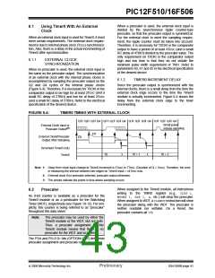
FIGURE 6-4:
TIMER0 TIMING WITH EXTERNAL CLOCK
Q1 Q2 Q3 Q4 Q1 Q2 Q3 Q4 Q1 Q2 Q3 Q4 Q1 Q2 Q3 Q4
Small pulse
misses sampling
External Clock Input or
(2)
Prescaler Output
(1)
External Clock/Prescaler
Output After Sampling
(3)
Increment Timer0 (Q4)
Timer0
T0
T0 + 1
T0 + 2
Note 1: Delay from clock input change to Timer0 increment is 3TOSC to 7TOSC. (Duration of Q = TOSC). Therefore, the error
in measuring the interval between two edges on Timer0 input = ±4TOSC max.
2: External clock if no prescaler selected; prescaler output otherwise.
3: The arrows indicate the points in time where sampling occurs.
When assigned to the Timer0 module, all instructions
writing to the TMR0 register (e.g., CLRF 1,
6.2
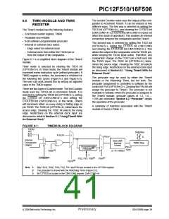
Prescaler
An 8-bit counter is available as a prescaler for the
Timer0 module or as a postscaler for the Watchdog
Timer (WDT), respectively (see Figure 10-12). For sim-
plicity, this counter is being referred to as “prescaler”
throughout this data sheet.
MOVWF 1, BSF 1, x, etc.) will clear the prescaler.
When assigned to WDT, a CLRWDTinstruction will clear
the prescaler along with the WDT. The prescaler is
neither readable nor writable. On a Reset, the
prescaler contains all ‘0’s.
Note:
The prescaler may be used by either the
Timer0 module or the WDT, but not both.
Thus, a prescaler assignment for the
Timer0 module means that there is no
prescaler for the WDT and vice-versa.
The PSA and PS<2:0> bits (OPTION<3:0>) determine
prescaler assignment and prescale ratio.
© 2006 Microchip Technology Inc.
Preliminary
DS41268B-page 41

 ETC [ ETC ]