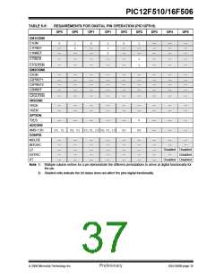
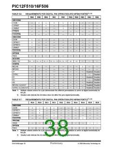
PIC12F510/16F506
The second Counter mode uses the output of the com-
parator to increment Timer0. It can be entered in two
different ways. The first way is selected by setting the
T0CS bit (OPTION<5>), and clearing the C1T0CS bit
(CM1CON0<4>) (C1OUTEN [CM1CON0<6>] does not
affect this mode of operation). This enables an internal
connection between the comparator and the Timer0.
6.0
TMR0 MODULE AND TMR0
REGISTER
The Timer0 module has the following features:
• 8-bit timer/counter register, TMR0
• Readable and writable
• 8-bit software programmable prescaler
• Internal or external clock select:
- Edge select for external clock
The second way is selected by setting the T0CS bit
(OPTION<5>), setting the C1T0CS bit (CM1CON0)
and clearing the C1OUTEN bit (CM1CON0<6>). This
allows the output of the comparator onto the T0CKI pin,
while keeping the T0CKI input active. Therefore, any
comparator change on the COUT pin is fed back into
the T0CKI input. The T0SE bit (OPTION<4>) deter-
mines the source edge. Clearing the T0SE bit selects
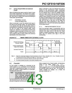
the rising edge. Restrictions on the external clock input
as discussed in Section 6.1 “Using Timer0 With An
External Clock”.
- External clock from either the T0CKI pin or
from the output of the comparator
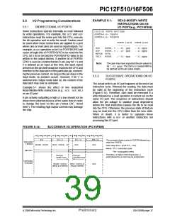
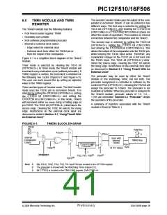
Figure 6-1 is a simplified block diagram of the Timer0
module.
Timer mode is selected by clearing the T0CS bit
(OPTION<5>). In Timer mode, the Timer0 module will
increment every instruction cycle (without prescaler). If
TMR0 register is written, the increment is inhibited for
the following two cycles (Figure 6-2 and Figure 6-3).
The user can work around this by writing an adjusted
value to the TMR0 register.
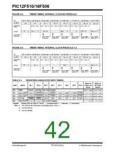
The prescaler may be used by either the Timer0
module or the Watchdog Timer, but not both. The
prescaler assignment is controlled in software by the
control bit PSA (OPTION<3>). Clearing the PSA bit will
assign the prescaler to Timer0. The prescaler is not
readable or writable. When the prescaler is assigned to
the Timer0 module, prescale values of 1:2, 1:4,...,
1:256 are selectable. Section 6.2 “Prescaler” details
the operation of the prescaler.
There are two types of Counter mode. The first Counter
mode uses the T0CKI pin to increment Timer0. It is
selected by setting the T0CKI bit (OPTION<5>), setting
the C1T0CS bit (CM1CON0<4>) and setting the
C1OUTEN bit (CM1CON0<6>). In this mode, Timer0
will increment either on every rising or falling edge of
pin T0CKI. The T0SE bit (OPTION<4>) determines the
source edge. Clearing the T0SE bit selects the rising
edge. Restrictions on the external clock input are
discussed in detail in Section 6.1 “Using Timer0 With
An External Clock”.
A summary of registers associated with the Timer0
module is found in Table 6-1.
FIGURE 6-1:
TIMER0 BLOCK DIAGRAM
T0CKI
Pin
Data Bus
FOSC/4
0
1
PSOUT
8
1
0
1
0
Internal
Comparator
Output
Sync with
Internal
Clocks
TMR0 Reg
Programmable
PSOUT
Sync
(2)
Prescaler
(1)
(2 TCY delay)
T0SE
3
(3)
(1)
(1)
C1T0CS
PS2, PS1, PS0
PSA
(1)
T0CS
Note 1: Bits T0CS, T0SE, PSA, PS2, PS1 and PS0 are located in the OPTION register.
2: The prescaler is shared with the Watchdog Timer (Figure 6-5).
3: Bit C1T0CS is located in the CM1CON0 register, CM1CON0<4>.
© 2006 Microchip Technology Inc.
Preliminary
DS41268B-page 39

 ETC [ ETC ]