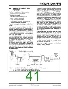
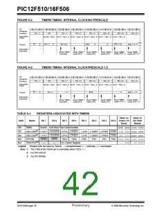
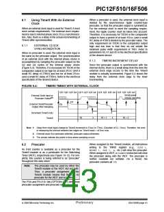
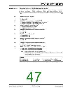
PIC12F510/16F506
To change prescaler from the WDT to the Timer0
module, use the sequence shown in Example 6-2. This
sequence must be used even if the WDT is disabled. A
CLRWDT instruction should be executed before
switching the prescaler.
6.2.1
SWITCHING PRESCALER
ASSIGNMENT
The prescaler assignment is fully under software
control (i.e., it can be changed “on-the-fly” during pro-
gram execution). To avoid an unintended device Reset,
the following instruction sequence (Example 6-1) must
be executed when changing the prescaler assignment
from Timer0 to the WDT.
EXAMPLE 6-2:
CHANGING PRESCALER
(WDT→TIMER0)
CLRWDT
;Clear WDT and
;prescaler
EXAMPLE 6-1:
CHANGING PRESCALER
(TIMER0 → WDT)
;Clear WDT
MOVLW ‘xxxx0xxx’ ;Select TMR0, new
;prescale value and
;clock source
CLRWDT
CLRF
TMR0
;Clear TMR0 & Prescaler
OPTION
MOVLW ‘00xx1111’b ;These 3 lines (5, 6, 7)
OPTION
;are required only if
;desired
CLRWDT
;PS<2:0> are 000 or 001
MOVLW ‘00xx1xxx’b ;Set Postscaler to
OPTION
;desired WDT rate
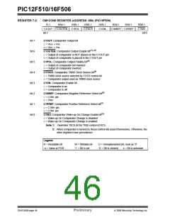
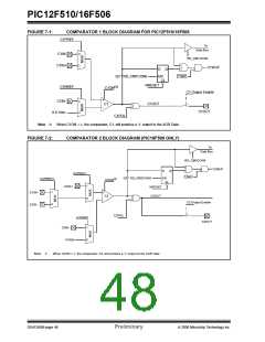
FIGURE 6-5:
BLOCK DIAGRAM OF THE TIMER0/WDT PRESCALER
(2)
T0CKI
Pin
TCY (= FOSC/4)
Data Bus
8
0
M
U
X
1
1
0
M
U
X
Comparator
Output
Sync
2
Cycles
1
TMR0 Reg
0
(1)
(1)
T0SE
T0CS
(1)
PSA
(3)
C1T0CS
0
1
8-bit Prescaler
M
U
X
8
Watchdog
Timer
(1)
8-to-1 MUX
PS<2:0>
(1)
PSA
1
0
WDT Enable bit
(1)
MUX
PSA
WDT
Time-Out
Note 1: T0CS, T0SE, PSA, PS<2:0> are bits in the OPTION register.
2: T0CKI is shared with pin GP2 on the PIC12F510 and shared with RC5 on the PIC16F506.
3: Bit C1T0CS is located in the CM1CON0 register.
DS41268B-page 42
Preliminary
© 2006 Microchip Technology Inc.

 ETC [ ETC ]