PIC12F510/16F506
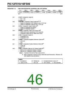
REGISTER 7-2:
CM1CON0 REGISTER (ADDRESS: 08h) (PIC16F506)
R-1
R/W-1
R/W-1
R/W-1
R/W-1
C1ON
R/W-1
R/W-1
R/W-1
C1WU
C1OUT C1OUTEN C1POL
bit 7
C1T0CS
C1NREF C1PREF
bit 0
bit 7
bit 6
bit 5
bit 4
bit 3
bit 2
bit 1
bit 0
C1OUT: Comparator Output bit
1= VIN+ > VIN-
0= VIN+ < VIN-
C1OUTEN: Comparator Output Enable bit(1), (2)
1= Output of comparator is NOT placed on the C1OUT pin
0= Output of comparator is placed in the C1OUT pin
C1POL: Comparator Output Polarity bit(2)
1= Output of comparator not inverted
0= Output of comparator inverted
C1T0CS: Comparator TMR0 Clock Source bit(2)
1= TMR0 clock source selected by TOCS control bit
0= Comparator output used as TMR0 clock source
C1ON: Comparator Enable bit
1= Comparator is on
0= Comparator is off
C1NREF: Comparator Negative Reference Select bit(2)
1= C1IN- pin
0= VREF
C1PREF: Comparator Positive Reference Select bit(2)
1= C1IN+ pin
0= C1IN- pin
C1WU: Comparator Wake-up On Change Enable bit(2)
1= Wake-up On Comparator Change is disabled
0= Wake-up On Comparator Change is enabled.
Note 1: Overrides T0CS bit for TRIS control of RC5.
2: When comparator is turned on, these control bits assert themselves. Otherwise, the
other registers have precedence.
Legend:
R = Readable bit
-n = Value at POR
W = Writable bit
‘1’ = Bit is set
U = Unimplemented bit, read as ‘0’
‘0’ = Bit is cleared x = Bit is unknown
DS41268B-page 44
Preliminary
© 2006 Microchip Technology Inc.

 ETC [ ETC ]