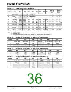
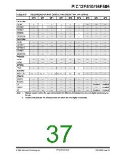
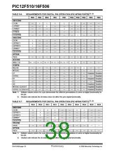
PIC12F510/16F506
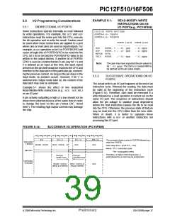
EXAMPLE 5-1:
READ-MODIFY-WRITE
INSTRUCTIONS ON AN
I/O PORT(e.g., PIC16F506)
5.5
I/O Programming Considerations
5.5.1
BIDIRECTIONAL I/O PORTS
Some instructions operate internally as read followed
by write operations. For example, the BCF and BSF
instructions read the entire port into the CPU, execute
the bit operation and re-write the result. Caution must
be used when these instructions are applied to a port
where one or more pins are used as input/outputs. For
example, a BSFoperation on bit 5 of PORTB/GPIO will
cause all eight bits of PORTB/GPIO to be read into the
CPU, bit 5 to be set and the PORTB/GPIO value to be
written to the output latches. If another bit of PORTB/
GPIO is used as a bidirectional I/O pin (say bit ‘0’) and
it is defined as an input at this time, the input signal
present on the pin itself would be read into the CPU and
rewritten to the data latch of this particular pin, overwrit-
ing the previous content. As long as the pin stays in the
Input mode, no problem occurs. However, if bit ‘0’ is
switched into Output mode later on, the content of the
data latch may now be unknown.
;Initial PORTB Settings
;PORTB<5:3> Inputs
;PORTB<2:0> Outputs
;
;
;
PORTB latch PORTB pins
----------
PORTB, 5 ;--01 -ppp
PORTB, 4 ;--10 -ppp
----------
--11 pppp
--11 pppp
BCF
BCF
MOVLW 007h;
TRIS
PORTB
;--10 -ppp
--11 pppp
;
Note:
The user may have expected the pin values to
be ‘--00 pppp’. The 2nd BCFcaused RB5 to
be latched as the pin value (High).
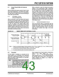
5.5.2
SUCCESSIVE OPERATIONS ON I/O
PORTS
The actual write to an I/O port happens at the end of an
instruction cycle. Whereas for reading, the data must
be valid at the beginning of the instruction cycle
(Figure 5-14). Therefore, care must be exercised if a
write followed by a read operation is carried out on the
same I/O port. The sequence of instructions should
allow the pin voltage to stabilize (load dependent)
before the next instruction causes the file to be read
into the CPU. Otherwise, the previous state of that pin
may be read into the CPU rather than the new state.
When in doubt, it is better to separate these
instructions with a NOP or another instruction not
accessing this I/O port.
Example 5-1 shows the effect of two sequential
Read-Modify-Write instructions (e.g., BCF, BSF, etc.)
on an I/O port.
A pin actively outputting a high or a low should not be
driven from external devices at the same time in order
to change the level on this pin (“wired OR”, “wired
AND”). The resulting high output currents may damage
the chip.
FIGURE 5-14:
SUCCESSIVE I/O OPERATION (PIC16F506)
Q1 Q2 Q3 Q4 Q1 Q2 Q3 Q4 Q1 Q2 Q3 Q4 Q1 Q2 Q3 Q4
PC + 3
PC
MOVWF PORTB
PC + 1
PC + 2
This example shows a write to PORTB followed by a
read from PORTB.
Instruction
Fetched
MOVF PORTB, W
NOP
NOP
Data setup time = (0.25 TCY – TPD)
where: TCY = instruction cycle
TPD = propagation delay
RB<5:0>
Therefore, at higher clock frequencies, a
write followed by a read may be problematic.
Port pin
written here
Port pin
sampled here
Instruction
Executed
MOVWF PORTB
MOVF PORTB,W
NOP
(Write to PORTB)
(Read PORTB)
© 2006 Microchip Technology Inc.
Preliminary
DS41268B-page 37

 ETC [ ETC ]