PIC12F510/16F506
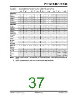
TABLE 5-6:
REQUIREMENTS FOR DIGITAL PIN OPERATION (PIC16F506 PORTB)(1), (2)
RB0
RB0
RB0
RB1
RB1
RB2 RB2 RB3
RB4
RB5
CM1CON0
C1ON
—
—
—
0
1
0
0
1
—
0
0
1
—
—
—
—
—
—
—
—
—
C1PREF
C1NREF
—
—
—
—
—
—
—
—
—
C1T0CS
—
—
—
—
—
—
—
—
—
—
—
—
—
—
—
—
—
—
—
C1OUTEN
CM2CON0
C2ON
1
1
0
—
—
—
—
—
—
—
—
—
—
—
—
—
—
—
—
—
—
—
—
—
—
—
—
—
—
—
—
—
—
—
—
—
—
—
—
C2PREF1
C2PREF2
C2NREF
1
—
C2OUTEN
OPTION
T0CS
—
—
—
—
—
—
—
—
00
—
—
—
—
—
—
—
—
—
—
—
—
—
—
—
ADCON0
ANS<1:0>
CONFIG
MCLRE
INTOSC
LP
00, 01 00, 01 00, 01 00, 01, 10 00, 01, 10 00
—
—
—
—
—
—
—
—
—
—
—
—
—
—
—
—
—
—
—
—
—
—
—
—
—
—
—
—
—
—
—
—
—
—
—
—
—
—
—
—
—
—
—
—
—
—
—
—
—
—
—
—
—
—
—
—
—
—
—
—
—
—
—
0
—
—
—
—
—
—
—
—
—
—
—
—
Disabled Disabled
Disabled
Disabled Disabled
Disabled
EXTRC
—
XT
EC
—
HS
Disabled Disabled
Disabled Disabled
Disabled Disabled
INTOSC CLKOUT
EXTRC CLOCKOUT
Note 1: Multiple column entries for a pin demonstrate the different permutations to arrive at digital functionality for
the pin.
2: Shaded cells indicate the bit status does not affect the pins digital functionality.
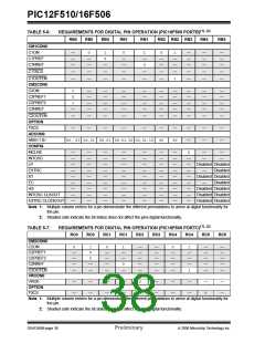
TABLE 5-7:
REQUIREMENTS FOR DIGITAL PIN OPERATION (PIC16F506 PORTC)(1), (2)
RC0
RC0
RC1
RC1
RC2
RC3
RC4
RC4
RC5
RC5
CM2CON0
C2ON
0
1
0
0
1
—
—
0
—
—
—
—
—
—
—
—
0
1
—
—
—
—
—
—
—
—
C2PREF1
C2PREF2
C2NREF
—
—
—
—
—
—
—
—
—
—
—
—
0
—
C2OUTEN
VRCON0
VROE
—
—
—
—
—
—
—
—
—
—
—
—
—
—
—
—
—
—
—
1
—
—
0
—
—
—
0
—
—
OPTION
T0CS
—
Note 1: Multiple column entries for a pin demonstrate the different permutations to arrive at digital functionality for
the pin.
2: Shaded cells indicate the bit status does not affect the pins digital functionality.
DS41268B-page 36
Preliminary
© 2006 Microchip Technology Inc.

 ETC [ ETC ]