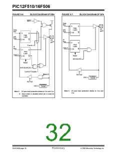
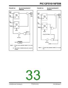
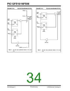
PIC12F510/16F506
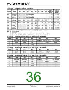
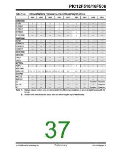
TABLE 5-1:
SUMMARY OF PORT REGISTERS
Value on
Power-On
Reset
Value on
All Other
Resets
Address
Name
Bit 7
Bit 6
Bit 5
Bit 4
Bit 3
Bit 2
Bit 1 Bit 0
(1)
N/A
TRISGPIO
—
—
—
—
I/O Control Register
I/O Control Register
I/O Control Register
--11 1111
--11 1111
--11 1111
1111 1111
1111 1111
--11 1111
--11 1111
--11 1111
1111 1111
1111 1111
(2)
N/A
TRISB
(2)
N/A
TRISC
—
—
(1)
N/A
OPTION
GPWU
RBWU
GPPU
RBPU
T0CS
T0CS
PA0
TOSE
TOSE
TO
PSA
PSA
PD
PS2
PS2
Z
PS1
PS1
DC
PS0
PS0
C
(2)
N/A
OPTION
(1)
(3)
03h
STATUS
GPWUF CWUF
RBWUF CWUF
0001 1xxx qq0q quuu
0001 1xxx qq0q quuu
(2)
(3)
03h
STATUS
PA0
TO
PD
Z
DC
C
(1)
06h
GPIO
—
—
—
—
—
—
GP5
RB5
RC5
GP4
RB4
RC4
GP3
RB3
RC3
GP2
RB2
RC2
GP1
RB1
RC1
GP0
RB0
RC0
--xx xxxx
--xx xxxx
--xx xxxx
--uu uuuu
(2)
06h
PORTB
--uu uuuu
--uu uuuu
(2)
07h
PORTC
Legend:
– = unimplemented read as ‘0’, x= unknown, u= unchanged, q= depends on condition.
Note 1: PIC12F510 only.
2: PIC16F506 only.
3: If Reset was due to wake-up on pin change, then bit 7 = 1. All other Resets will cause bit 7 = 0.
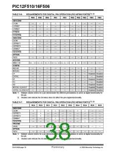
TABLE 5-2:
I/O PIN FUNCTION ORDER OF PRECEDENCE (PIC16F506)
Priority
RB0
AN0/C1IN+
TRISB
—
RB1
AN1/C1IN-
TRISB
—
RB2
C1OUT
AN2
RB3
RB4
RB5
OSC1/CLKIN
TRISB
1
2
3
Input/MCLR OSC2/CLKOUT
—
—
TRISB
—
TRISB
—
TABLE 5-3:
Priority
I/O PIN FUNCTION ORDER OF PRECEDENCE (PIC16F506)
RC0
RC1
RC2
RC3
RC4
RC5
1
2
C2IN+
TRISC
C2IN-
CVREF
TRISC
TRISC
—
C2OUT
TRISC
T0CKI
TRISC
TRISC
TABLE 5-4:
Priority
I/O PIN FUNCTION ORDER OF PRECEDENCE (PIC12F510)
GP0
AN0/C1IN+
TRISIO
—
GP1
AN1/C1IN-
TRISIO
—
GP2
C1OUT
AN2
GP3
GP4
OSC2
TRISIO
—
GP5
OSC1/CLKIN
TRISIO
—
1
2
3
4
Input/MCLR
—
—
—
T0CKI
TRISIO
—
—
—
—
DS41268B-page 34
Preliminary
© 2006 Microchip Technology Inc.

 ETC [ ETC ]